

 NinjaCalc
Discrete Current Sources

Discrete current sources are constant-current circuits built from just a transistor and a handful of passive components (e.g. no op-amp or other more “advanced” circuitry). They set a fixed current and are commonly used for biasing and simple LED drives. This page covers two popular discrete designs: the Zener diode + BJT source and the JFET constant-current diode.
For the general concept of current sources and sinks (compliance, schematic symbols, independent vs. controlled sources) see the parent Current Sources And Sinks page. Current-mirror-based sources are covered separately on the Current Mirrors page.
Zener Diode And BJT Current Source
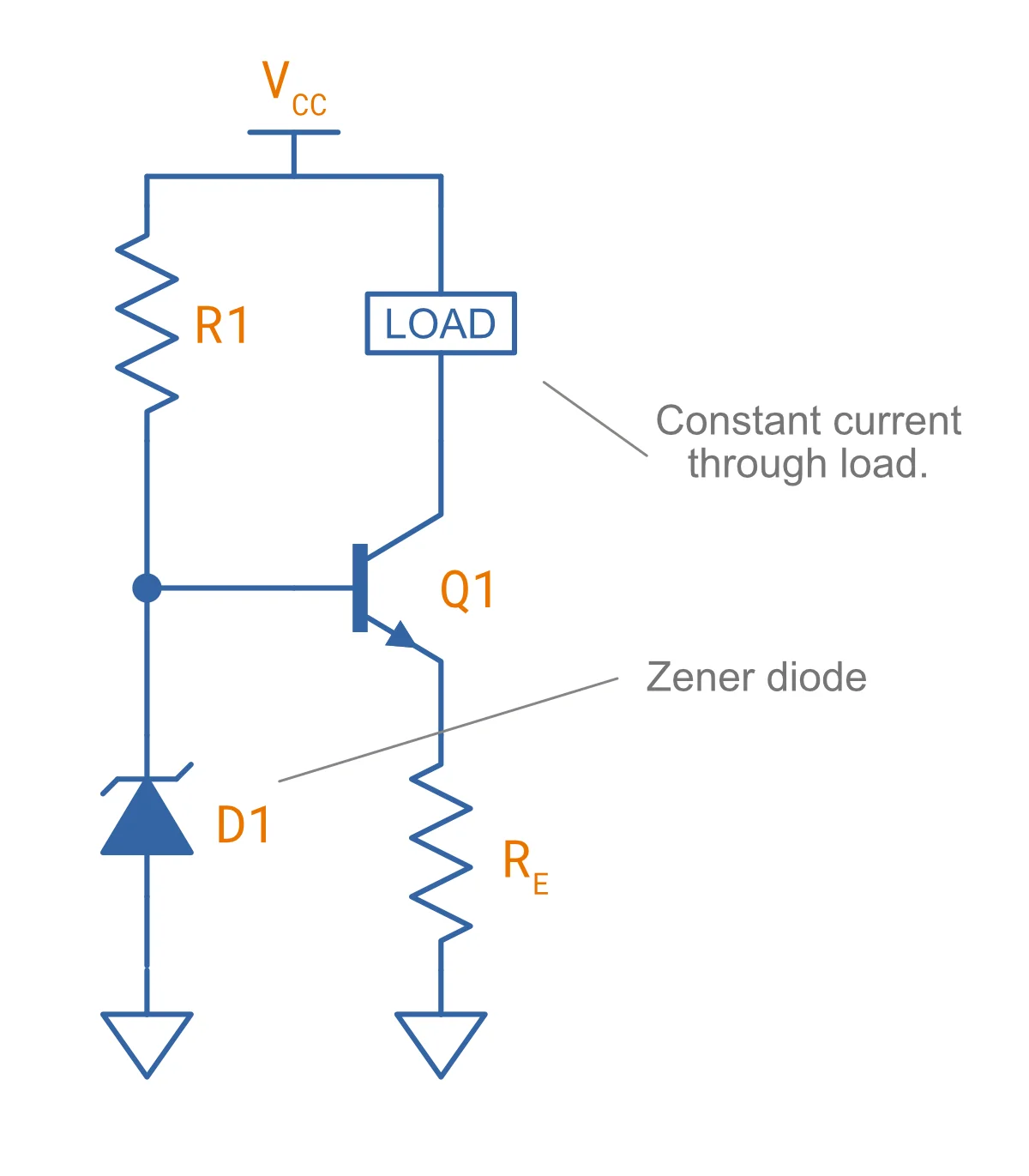
Below shows one of the popular methods for constructing a current source from a Zener diode and BJT.
How It Works
- The Zener diode , biased into its voltage regulation range with resistor , maintains a steady voltage at the base of the BJT transistor.
- Using the rule that there is a drop across the base-emitter junction of a BJT, this puts a fixed voltage at the emitter also.
- Since this means there is a fixed voltage across , this means by Ohm’s law there is a fixed current through .
- Because most of the current supplied to the emitter of a BJT comes from the collector (only about th to th of the current comes from the base, depending on the gain of the BJT), this means there is a fixed current through also!
The current through the load is given by:
where:
is the voltage of the Zener diode in
is the resistance of resistor in
is the resulting current through the load resistor, in
Double-Diode And BJT Current Source
This design is similar to the Zener diode and BJT current source above, but uses two diodes in series instead of a Zener diode. This time, rather than sinking current from a load down to ground, we’ll build a high-side current source that pushes current into the load — so we’ll use a PNP transistor above the load. The following schematic shows a current source that will drive approx. into a load:
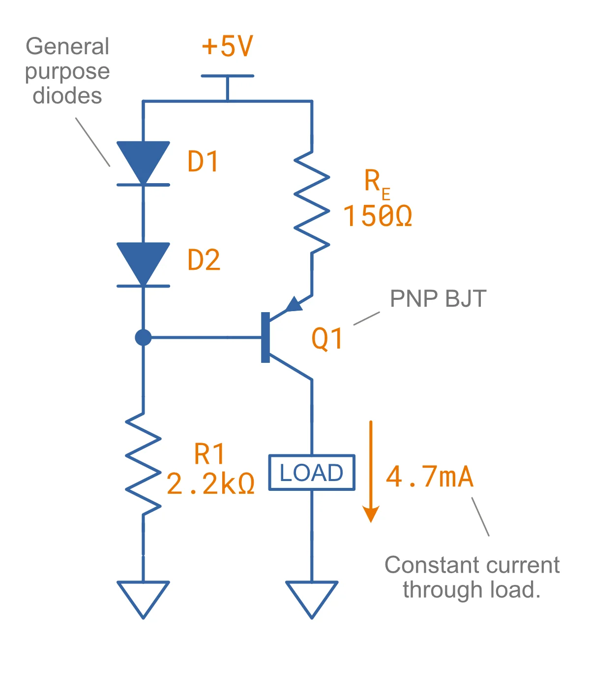
This works because there is across and . There is a drop of across the base-emitter junction of the PNP transistor, so there is of drop across . The current through is then . Because the base current of the PNP transistor is small compared to the collector current, this means the current through the load will also be approx. .
The exact value of does not matter, as long as there is enough current to properly forward bias the diodes but not too much to overheat them.
Two-BJT Current Sink
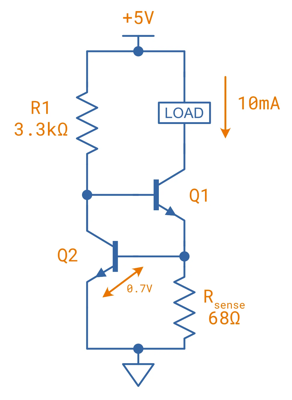
The two-transistor current sink (also called the two-transistor current limiter) is another popular discrete current source. Unlike the Zener and double-diode designs above, this circuit does not use Zeners or diodes as a voltage reference. Instead, it uses a second BJT to limit the current through the first BJT. It has the advantage of being able to work down to very low voltage and uses two of the same component (the BJTs).
How It Works
is the pass transistor that carries the load current, and feeds base current into it from the top rail. The sense resistor sits in ‘s emitter, so the entire load current flows through it. The clever part is : its base-emitter junction is connected directly across , and its collector is tied to ‘s base.
The loop regulates itself against ‘s base-emitter voltage:
- As the load current rises, the voltage across rises with it.
- When that voltage reaches ‘s turn-on threshold (≈), begins to conduct.
- pulls ‘s base voltage down, stealing base drive from and throttling it back.
- The loop settles at the point where drops almost exactly ≈.
The load current is therefore set by the sense resistor and a single base-emitter voltage:
where:
is the base-emitter voltage of , in
is the resistance of the sense resistor, in
is the resulting current through the load, in
Because the reference is a single, well-defined rather than a loosely-toleranced Zener voltage, the absolute accuracy is reasonable. However, drifts by about , so the current has a positive temperature coefficient (roughly for a sense drop).
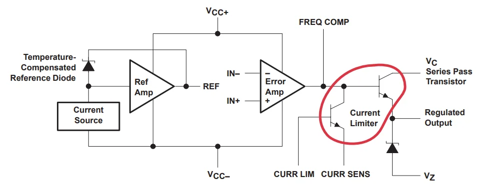
What makes the two-BJT topology notable is that it is likely the most commonly used circuit purely as a current limiter: it normally passes current freely and only intervenes on overload, e.g. a short-circuit protection front-end on power supplies.
Constant-Current Diode (JFET Current Source)
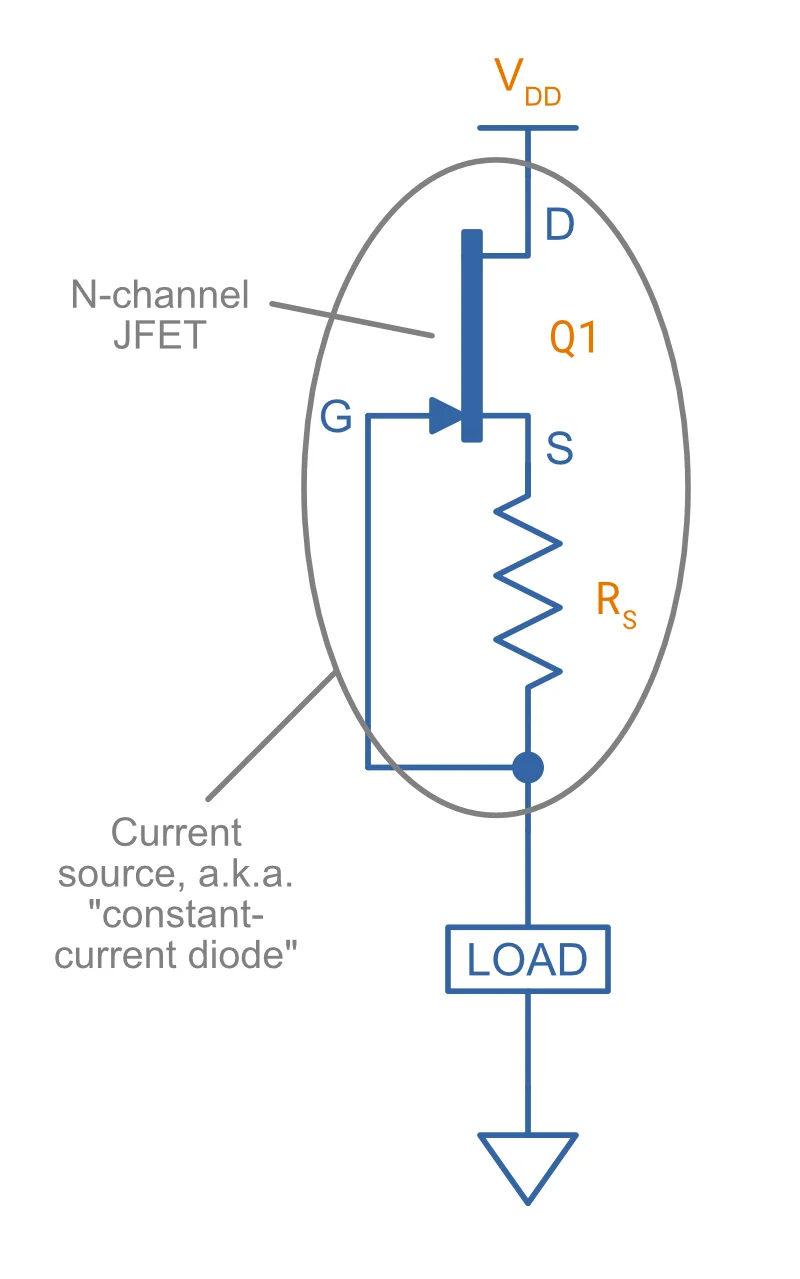
The constant-current diode (a.k.a JFET current source, current-limiting diode (CLD), or regulating diode2) is a very simple current source made from a JFET and optional resistor.
Below shows the schematic for a constant-current diode:
How It Works
The constant-current diode works by using the resistor to negatively bias the N-channel JFET at a specific operating point. At this operating point the current from drain to source (and consequentially the load) will be relatively constant.3
How To Calculate The Value Of The Resistor
-
Decide on what N-channel JFET you are going to use and your desired constant current, .
-
You then calculate the required gate-source voltage5:
where:
is the gate-source voltage required to bias the JFET at the correct current, in
is the gate-source cutoff voltage, a parameter you can get from the JFETs datasheet, in
is the current you want the current source to drive at, in
is the zero gate-source drain current, a parameter you can get from the JFETs datasheet, in
is the conduction parameter for the JFET, and depends on the device geometry. This is not normally mentioned in the datasheet, however for this equation you can generally assume it to be . -
You can then find the value of with:
An important parameter determining the accuracy/stability of a constant-current diode is the output conductance of the JFET. This is the ratio of change in to change in . This is a measure of how stable the constant-current source will be to changes in the voltage across it, which occur if either the supply voltage or load resistance changes. The lower the the better (an ideal current source would have , which is the equivalent to a resistance of ).
For more great reading on the constant-current diode, see the Vishay/Siliconix application note AN103.5
Depletion-Mode MOSFET Current Source
A depletion-mode MOSFET can be turned into a two-terminal constant-current source in exactly the same way as the JFET constant-current diode above. Unlike the far more common enhancement-mode MOSFET (which needs a gate-source voltage above a threshold before it conducts), a depletion-mode MOSFET is normally on — it conducts at . This means it can be self-biased with a single source resistor, just like the JFET.
The attraction over a JFET is voltage and power headroom. Where JFET constant-current diodes top out around and , depletion-mode MOSFETs built for this job go much higher. The classic part is the Supertex (now Microchip) DN2540, a , device6; the LND150 pushes the voltage rating higher still. These are widely used for high-voltage LED strings, vacuum-tube plate loads, and high-voltage startup/bleeder supplies.
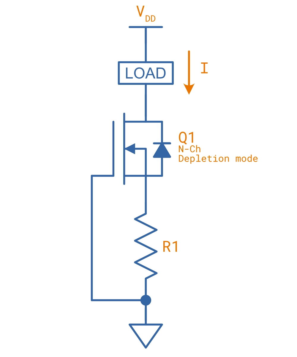
How It Works
Self-biasing works identically to the constant-current diode: the source resistor develops a voltage as the drain current flows through it, and because the gate is tied to the bottom of this appears as a negative gate-source voltage. As the current rises, becomes more negative and pinches the channel back, settling at a constant operating current.
How To Calculate The Value Of The Resistor
The depletion MOSFET follows the same square-law relationship as the JFET, so the design steps are identical:
-
Choose your depletion-mode MOSFET and desired constant current, .
-
Calculate the required gate-source voltage:
where the parameters mean the same as in the JFET section above ( is the gate-source cutoff voltage, the zero-gate-voltage drain current, and ).
-
Find with:
Comparison Of The Discrete Topologies
The table below summarizes the three discrete current sources covered on this page to help you pick between them.
| Property | Zener + BJT | JFET Constant-Current Diode | Depletion-Mode MOSFET |
|---|---|---|---|
| Terminals | 3 (referenced to a rail) | 2 (floating, not rail-referenced) | 2 (floating, not rail-referenced) |
| Typical current range | mA up to amps (limited by BJT and power) | (e.g. DN2540) | |
| Max voltage | Set by BJT (tens of volts typical) | + (e.g. DN2540) | |
| Accuracy (untrimmed) | Moderate — set by and the approximation | Poor — large spread | Poor — large spread (2:1) |
| Temperature stability | Good if tempco offsets (≈) | Good | Moderate (≈ for DN2540) |
| Parts count | Higher (Zener, bias resistor, BJT, ) | Lowest (JFET + optional resistor) | Low (MOSFET + resistor) |
| Best for | Adjustable higher-current biasing off a rail | Simple low-power floating current limiting | High-voltage / higher-power floating sources |
For anything requiring accuracy, all three benefit from a trimmer to set the current by measurement, as discussed in the sections above.
Source Resistor Calculator
The calculator below sizes for either device type. Enter the datasheet , the range, and your target current — it returns the resulting range and a suggested fixed-resistor-plus-trimmer combination. The presets load the datasheet values for the parts discussed above.
R_S for a JFET or depletion-mode MOSFET wired as a two-terminal constant-current source. Because the cutoff voltage V_GS(off) is specified as a datasheet range, the result is a range of R_S. One solution is to pick a fixed value near the low end and trim up with a series potentiometer.Footnotes
-
Texas Instruments (1999, Jul). µA723 Precision Voltage Regulators [datasheet]. Retrieved 2026-07-18, from https://www.ti.com/lit/ds/symlink/ua723.pdf. ↩
-
Central Semiconductor Corp. What is a Current Limiting Diode?. Retrieved 2022-01-11, from https://www.centralsemi.com/pdfs/selection/leaded/what_is_a_cld.pdf. ↩
-
Electronics Tutorials. FET Current Source. Retrieved 2022-01-11, from https://www.electronics-tutorials.ws/transistor/fet-current-source.html. ↩
-
On Semiconductor (now On Semi) (2010, Feb). 2N5457, 2N5458 JFETs: General Purpose N−Channel − Depletion [datasheet]. Retrieved 2022-01-11, from https://www.onsemi.com/pdf/datasheet/2n5457-d.pdf. ↩
-
Siliconix (now Vishay) (1997, Mar 10). AN103: The FET Constant-Current Source/Limiter [application note]. Retrieved 2021-04-29, from https://www.vishay.com/docs/70596/70596.pdf. ↩ ↩2
-
Supertex (now Microchip). DN2535/DN2540 N-Channel Depletion-Mode Vertical DMOS FETs [datasheet]. Retrieved 2026-07-15, from https://cdn-reichelt.de/documents/datenblatt/A200/DN240N5-G-STEX.pdf. ↩ ↩2 ↩3