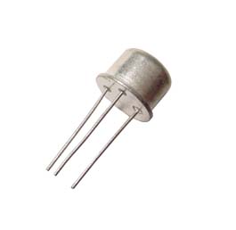
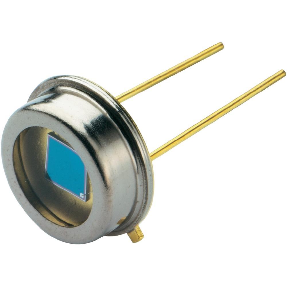
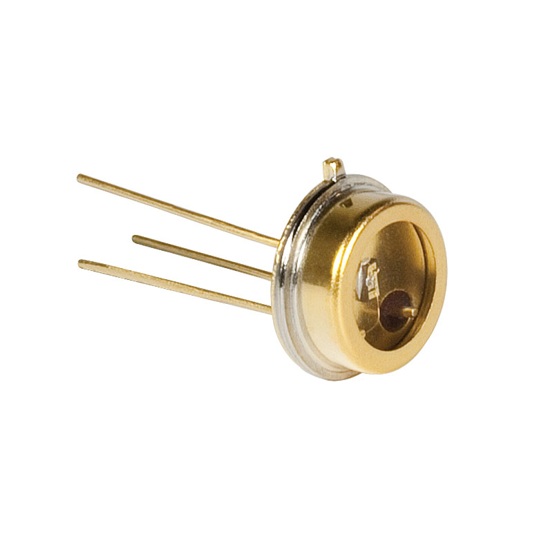
TO-39 Component Package

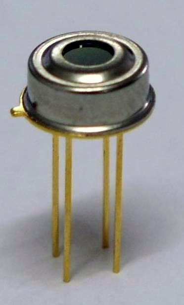
The TO-39 (Transistor Outline 39) package is a family of metallic can packages used for hermetically sealing semiconductor devices. It usually has three legs (the TO-39-3 variant), but variants with up to 10 legs are in use. The metal case can be gold coated. As a large through-hole package, it is being used less in recent years, although it still finds applications with high-end, sensitive electronic devices such as UV LEDs and IR thermometers.
Synonyms:
TO-205AD(TO-39-3)H(Linear Technology Package Code)
Variants:
- TO-39-3
- TO-39-4
- TO-39-6
- TO-39-8
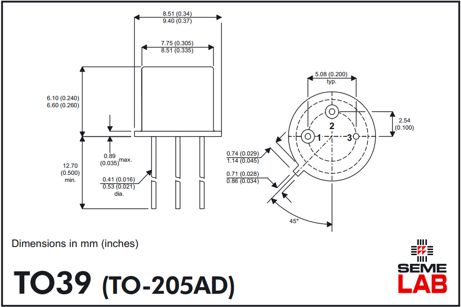
Pin Count: 3-10 (most common pin count is 3)
Pitch: 2.54mm (100mil)
Common Uses:
- Transistors
- UV LEDs
- IR Thermometers
Similar To:
- TO-3
- TO-18
Thermal Resistance:
- (mounted in the standard way to the PCB)
Typical PCB Land Area: (smallest square area to enclose package)
3D Models: 3dContentCentral
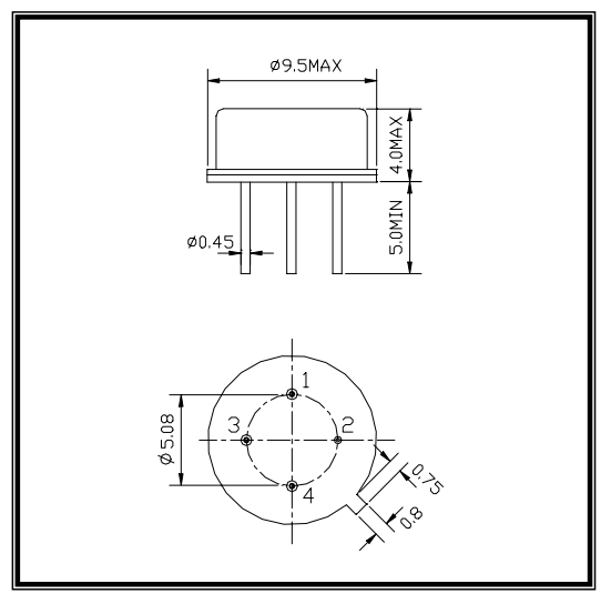
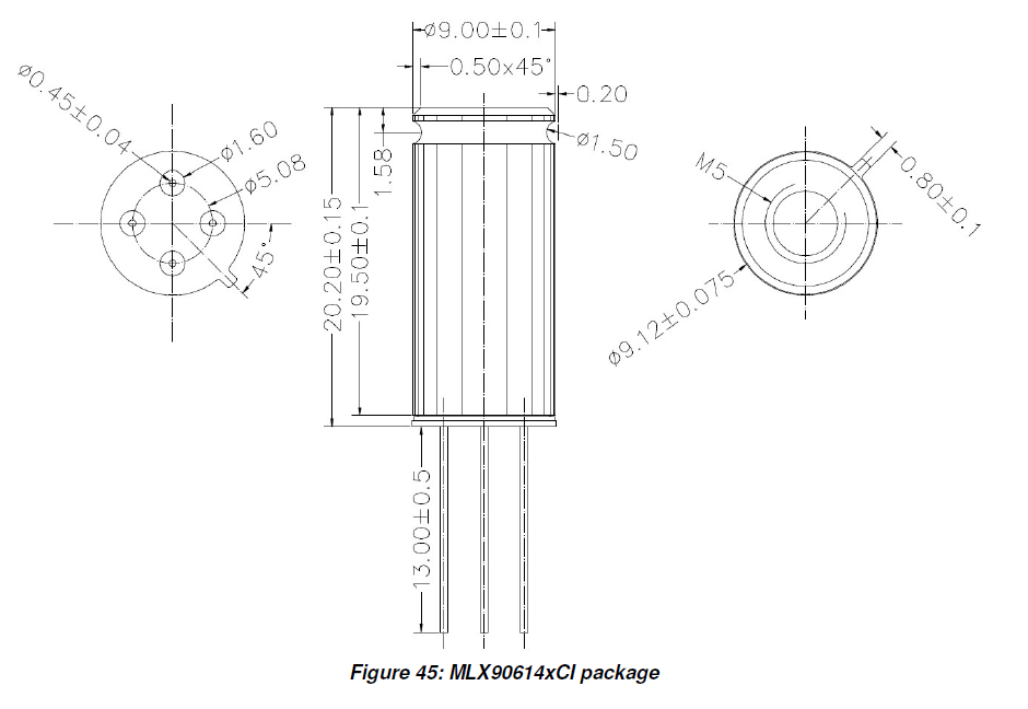
The TO-39 package has a small polarising tab on the side of the metal case. However this is merely an indication and does not prevent the user from inserting the package incorrectly. The 3-pin variant can only be inserted in one way because it’s 3 pins are not symmetric around the centre (it’s the same as the 4-pin version, but with one pin missing).
The TO-39 package comes in different heights, two of which are commonly called low profile and high profile.
The ground pin of the `TO-39 package is usually connected to the metal case. The TO-39 can sit directly on the PCB, so it’s important to consider that it could short out any unmasked nets running underneath the package. This also applies to the pads surrounding the non-ground pins. I measured the clearance around the non-ground pins and the maximum diameter of the pad surrounding the hole was about 1.60mm before it would short to ground. The pad on the other side of the PCB can be as large as you want.
You can get clip-on heatsinks for the TO-39 package with thermal resistances of around , which drops the to around .
TO-39-2
TO-39-3
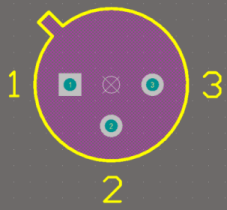
TO-39-4
TO-39 Ball Lens
Optan produces components which come in a TO-39 “Ball Lens” package.

Footnotes
-
Optan (2021). Products. Retrieved 2021-11-08, from https://www.optanled.com/products. ↩