Charge Pumps

A charge pump (also known as a Dickson charge pump, switched capacitor circuit, voltage multiplier, or voltage splitter when halving the input voltage) is a voltage-converting circuit that uses capacitors, diodes, and an oscillating switch to move charge from one capacitor to another. Like a boost converter, charge pumps are typically used to produce an output voltage which is higher than the input voltage. However, they can also be configured to reduce the input voltage (buck) or invert it.
The basic principle of a charge pump is to charge capacitors individually (in parallel) from the input voltage, and then connect them in series to provide a higher output voltage. Whilst this can be done manually or mechanically, almost every practical charge pump circuit uses electronic switches (diodes, MOSFETs, etc.) to change between series and parallel connectivity.
| Charge Pump | Boost Converter |
|---|---|
| Efficient at low power (<10mA) | Efficient at high power (>100mA) |
| Simple circuit, low component count | Complex control, high count/bulky components |
| Low noise | High noise |
A single capacitor/diode configuration (with additional smoothing capacitor on the output) doubles the input voltage. Multiple elements can be connected together to create larger voltage increases. Basic charge pumps that double/halve the input voltage are called unregulated charge pumps. There are also more advanced regulated charge pumps, which provide a fixed output voltage over a range of input voltages.
Marx generators are similar to charge pumps except they use spark gaps instead of diodes as the switching elements. Marx generators are typically used for high voltage/high power applications.
Charge pumps are very closely related to Switched-Capacitor Circuits.
How It Works
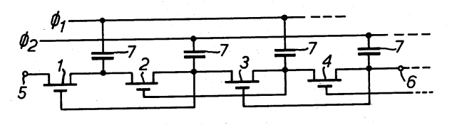
In charge pump designs in which both legs of the capacitor are switched to different parts of the circuit at the same time, the capacitors are called flying capacitors, named because both their leads are for a brief moment in time disconnected from the circuit. The capacitor connected across the output load is called the reservoir capacitor, storage capacitor or load capacitor.1
Schottky diodes are preferred because of their low forward voltage drop and higher switching speeds.
Larger reservoir capacitances result in longer start-up times, but result in less voltage ripple.
The switching frequency is usually limited to 100-500kHz.
MOSFETs can be wired to behave like a diode and are sometimes used instead of Schottky diodes. However the MOSFET-based charge pumps do not work as well at low voltages due to the large drain-source voltage drops across the MOSFETs.
Charge Pump Topologies
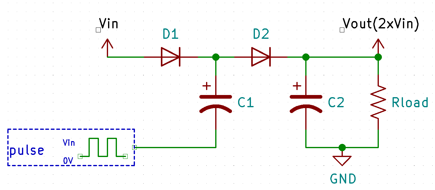
Basic Voltage Doubling Charge Pump
This is the most basic type of charge pump. We’ll go through each step of the process to show how exactly charge is moved around to have the effect of doubling the input voltage. This concept of “shunting around” charge (hence the pump part in the name) is the key concept of any charge pump topology.
- When voltage is first applied to the circuit, provides current through D1 and D2 and charges up both C1 and C2 to almost 5V, except C1 sees one forward voltage drop (300mV, using Schottky diodes) across D1 and C2 two forward voltage drops across D1 and D2.
- Then the pulse input transitions from 0V to 5V. Because C1 is already charged to 4.7V, and this 5V appears on the capacitors negative lead, it “pushes” the top lead of C1 up to 9.7V. This then causes a current from C1, through D2, into C2, charging it up past 5V.
- The pulse then transitions back to 0V, and the cycle begins again with C1 charging back up to 5V (remember that it would have dropped to somewhere between 0-5V when transferring charge to C2 in the previous step).
- After enough cycles, the output voltage on C2 stabilizes to . Note that here is the forward drop at the actual operating current, not the low-current 300mV figure quoted above --- under load the drop is larger, which is why the simulation below settles closer to 8.7V than the 9.4V the 300mV figure would suggest.
To demonstrate the behaviour of this circuit, I simulated it using KiCad and ngspice. The simulation files can be downloaded below:
The following KiCad schematics were used to perform the simulation:
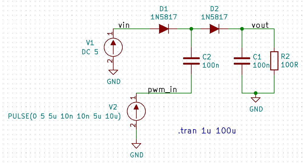
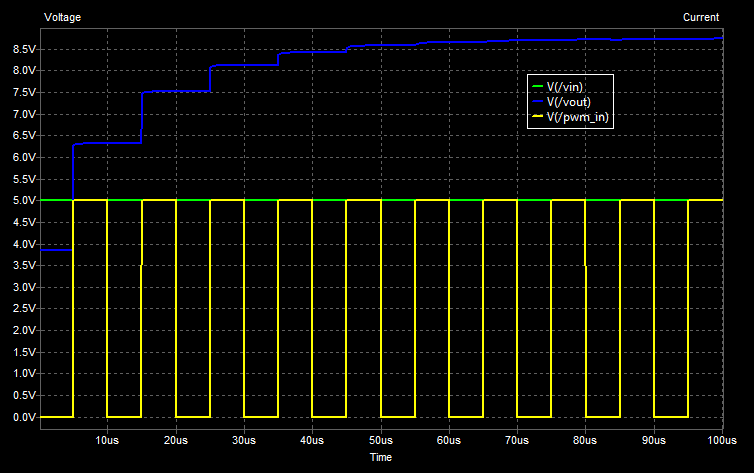
The below figure shows the behaviour of the voltage doubling charge pump. Notice that after about 5 cycles the output voltage stabilizes to its steady state value of approximately 8.7V. This simulation assumed a perfect voltage source driven pulse input, in reality the pulse input has some non-zero output impedance which affects the stabilization time and output current capacity.
Output Impedance
Charge pumps can be used as voltage sources, although normally only for light loads, as they generally have significant output impedance (compared to linear regulators and SMPS). In general, the output impedance for a charge pump can be calculated by2:
where:
is the output resistance, in Ohms []
is the number of stages, excluding the last “tank” capacitor
is the switching frequency, in Hertz []
is the capacitance of each stage, assuming they all have the same value, in Farads []
For more information on how this equation is derived, see the Switched Capacitor Circuits page.
Let’s compare what this equation says compared to a simulation. Below is the schematic of a Micro-Cap +3.3V voltage-doubling charge pump simulation. The input is driven with a 10kHz +3.3V square wave.
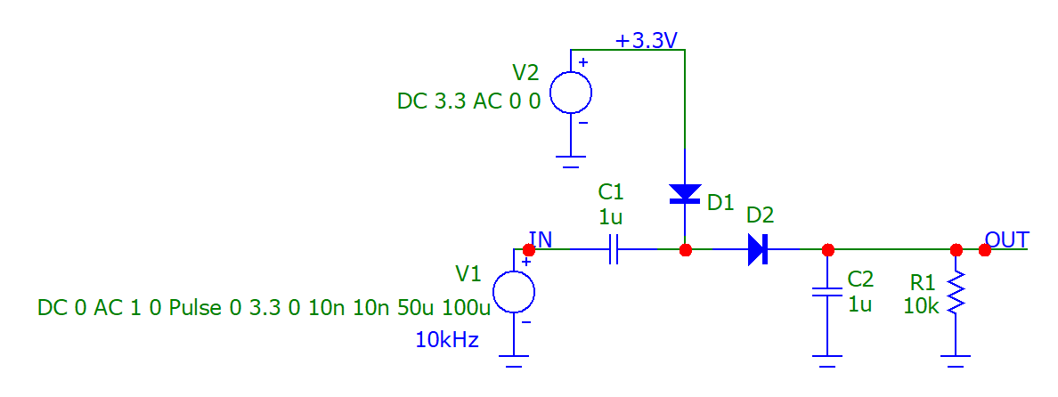
The equation predicts the output impedance to be:
To find the output impedance, I found the output voltage under no load, and the output voltage and current with a load. Both of these were done using transient-style simulations.
At no load, .
With , .
Thus we can find the output resistance using the resistor divider equation:
Re-arrange for :
So predicted by the equation and measured in the simulation. The measured value is higher, which is exactly what we’d expect: the equation gives the ideal output impedance (the “slow-switching limit”), accounting only for the charge transferred per cycle. It ignores the real losses in the circuit --- the diode forward voltage drops, the diode series resistance, and capacitor ESR --- all of which add to the output impedance. So the equation should be treated as a lower bound, with the real value sitting somewhat above it.
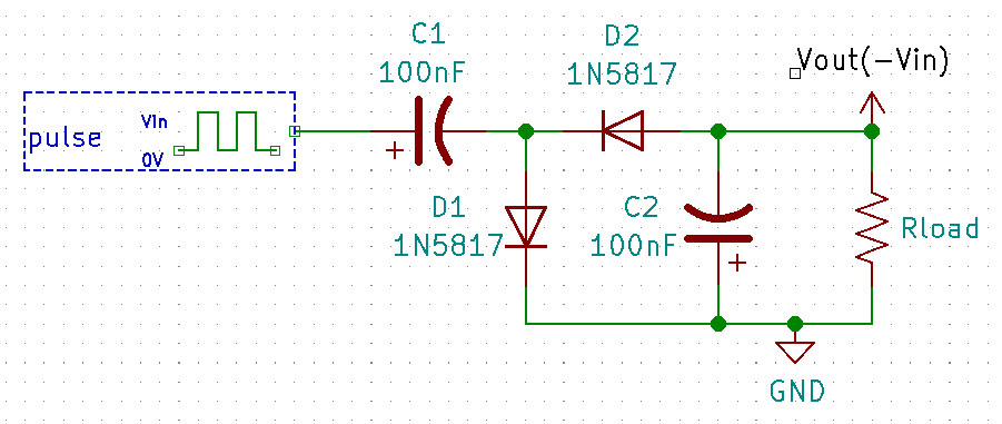
Voltage Inverting Charge Pump
Notice how while the voltage doubling charge pump requires two inputs ( and ), a voltage inverting charge pump only requires one --- .
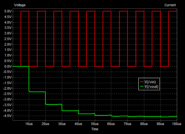
The simulation results:
History
The Greinacher voltage multiplier (a.k.a. half-wave doubler) was invented by Swiss physicist Heinrich Greinacher in 1919.3
John F. Dickson patented what is known as the “Dickson charge pump” in the late 1970’s (filed in 1978, patent dated July 22, 1980).4 It is very similar to the Greinacher doubler except it runs off a DC input. It was primarily used to generate programming/rewrite voltages in EEPROM/flash memory ICs.
Uses
Negative Voltage Bias For Op-Amps
Charge pumps can be used to provide the negative voltage to op-amps. They suit this application since op-amp power supplies typically require little current (1-20mA), and can generate the negative voltage from the main, higher-current, positive power source.
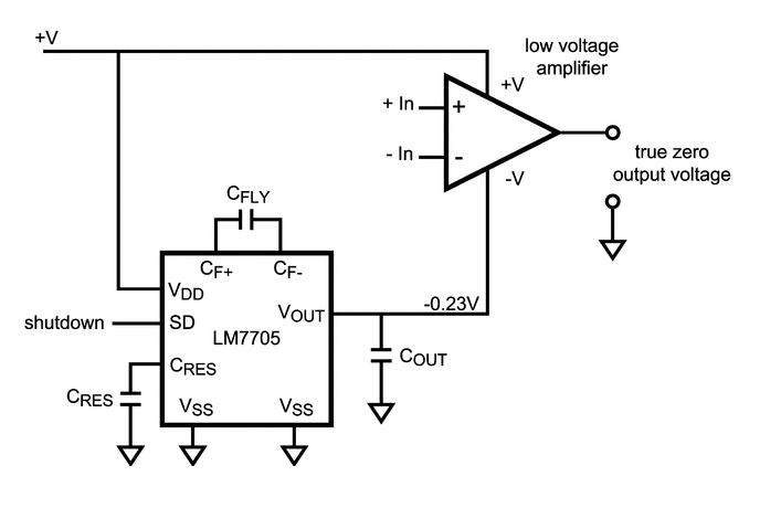
Special charge pumps exist that only produce a very small negative voltage (e.g. -250mV), for providing the negative power supply to rail-to-rail “single-supply” op-amps so that they can output a true 0V. More on this on the Op-amps page.
LED Drivers
Some LED drivers feature charge pumps to boost the supply voltage to a proper level to drive the LEDs. Charge pumps are usually featured in low power (20mA per channel) LED drivers, that may need to boost say, a +3.3V supply to +4.5V to drive an LED with the correct current. The NCP1840 8-Channel Charge-Pump I2C LED Driver by On Semiconductor is one such example.
MOSFET Gates
N-channel MOSFETs are typically better performing (lower , larger max. current limit) than P-channel MOSFETs. However, N-channel MOSFETs require a positive gate-source voltage () to turn them on. This makes it problematic to use them as a high-side switch on a circuit, as you require a voltage on the gate which is higher than the load/input voltage (the load is connected to the source, which is at the same potential as the input voltage when the switch is on).
The most common way to overcome this problem is to use a small charge pump circuit to power the gate. Many buck converters use this trick to use an N-channel rather than a P-channel MOSFET as the switching element.
RS-232
The RS-232 standard mandates 5-15V and levels. Because most modern day circuits are powered by +3.3 or +5V, charge pumps are commonly used to provide these higher voltage levels. Early RS-232 transceivers used unregulated charge pumps (which just doubled the input voltage), whilst more modern transceivers use regulated charge pumps which provide stable RS-232 logic levels over a range of input voltages.
Footnotes
-
Sipex Corporation (2006, Jul 24). ANI-19: Selecting Charge Pump Capacitors [application note]. Sipex Corporation. Retrieved 2020-12-14, from https://www.maxlinear.com/appnote/ani-19_selectingchargepumpcaps_072406_d.pdf. ↩
-
StackExchange: Electrical Engineering. Charge pump output resistance [forum post]. Retrieved 2022-09-14, from https://electronics.stackexchange.com/questions/136860/charge-pump-output-resistance. ↩
-
Jeff Sorensen (2020, Jun 30). Capacitive voltage conversion, aka the charge pump [article]. EDN. Retrieved 2020-12-08, from https://www.edn.com/capacitive-voltage-conversion-aka-the-charge-pump/. ↩
-
Justia. John F. Dickson Inventor Patents [patent search]. Justia Patents. Retrieved 2020-12-14, from https://patents.justia.com/inventor/john-f-dickson. ↩