Logic Families

Logic families are groups of basic digital logic electronic circuits (and, or, nor gates etc.), where each group consists of a different semiconductor technology from which the logic gates are built from. Within a family the voltage levels and signalling should be compatible between the various inputs and outputs.
This page covers high-level information about logic families that is useful when using them in circuit design. If you are interested in how the gates in the logic families are actually constructed, see the Digital Logic -> Gates page.
Logic families are sorted in alphabetical order. Take note that there may be a low-voltage equivalent of many signal types under the prefix “LV” (e.g. TTL and LVTTL).
CML
See PECL.
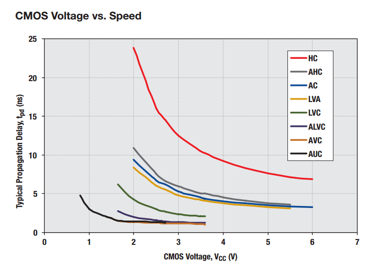
CMOS
Overview
CMOS (complementary metal-oxide semiconductor) is the most widespread logic family in use today. CMOS logic is built from P-channel (PMOS) and N-channel (NMOS) MOSFETs.
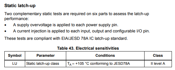
Latch-up
CMOS logic suffers from a phenomenon known as latch-up. This is when a short occurs between a power-rail and ground in a CMOS-based IC, usually causing serious operation problems if not destruction of the IC. Once latch-up is triggered, it cannot be removed until the circuit is power-cycled.
Latch-up occurs because the PN junctions that form the PMOS and NMOS switching elements form parasitic PNPN thyristors (SCRs)1. A latch-up has to be initially triggered by an over-voltage/current condition which causes the voltage on a pin to go at least one diode drop above the rail voltage, or one voltage drop below the ground.

Hot-plugging can cause latch-up issues.
ICs are sometimes tested against the EIA/JESD 78A IC latch-up standard and the IC is provided with a latch-up class. The tests involve:
- Applying a supply overvoltage condition to the ICs power pins
- A current injection to the ICs I/O pins
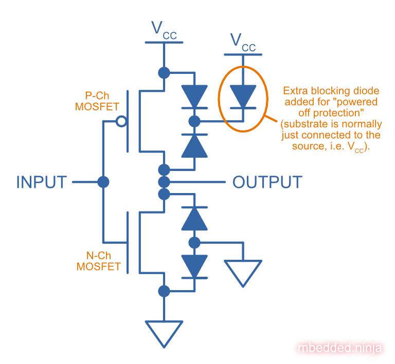
Powered Off Protection
By default, most CMOS based devices contain diodes from the I/O pins to the voltage rails and ground (this is an inherent part of the fabrication of a MOSFET and the intrinsic body diodes). Additional ESD protection diodes may be also added in parallel. Whilst normally a good thing, these diodes can cause problems, notably a problem called backfeeding. If the local power rail collapses, but signals are still present on the I/O pins (from other parts of the circuitry which are still powered), the diode from the I/O pin to will conduct and keep the power rail “propped up”.
Some logic gates include “powered-off protection” to prevent this, and allow external signals to be present when the power rail is at . Texas Instruments calls this protection23. The figure below shows how the standard CMOS totem-pole driver is modified to provide “powered-off protection”.
Some examples of ICs with “powered-off protection” include the SN74LVC1G125: Single Bus Buffer Gate With 3-State Output, the SN74CB3Q3125: 3.3-V, 2:1 (SPDT), 4-channel FET bus switch and the ADG5248F: 8:1 Analog Multiplexers.
AUC
Advanced ultra-low CMOS (AUC) is a CMOS logic family. It is optimised for 1.8V operation and voltage tolerant up to 3.6V.
LVCMOS
Voltage specifications:
| Parameter | Minimum | Typical | Maximum |
|---|---|---|---|
| 2.3V | 2.5V | 2.7V | |
| - | - | - | |
| - | - | - | |
| 1.7V | - | 3.6V | |
| -0.5V | - | 0.7V | |
| 1.9V | - | - | |
| - | - | 0.4V | |
| -12mA | - | - | |
| 12mA | - | - |
CSEF
See PECL.
CSL
See PECL.
DCS (Differential Current Switch)
DTLL (Differential Transistor-Transistor Logic)
DTLL is a differential signal type that is similar to standard TTL. Because of its differential nature, DTLL is preferred over TTL for communications over long cables. DTLL comes under the category HVDS (high-voltage differential signalling), and is the most popular choice in this category.
LVTTL
LVTTL is the low-voltage version of TTL.
Common drive-strengths are 24mA.
Converters
TI SN65LVELT23 converts LVPECL and LVDS to LVTTL.
LVDS
Stats
| Mode | Differential |
|---|---|
| Logic High () | 1.55V (+3.5mA through 100Ω) |
| Logic Low () | 0.95V (-3.5mA through 100Ω) |
| Common-mode Voltage () | 1.20V |
| Power () | 8.75mW (@ ) |
Because the current is kept constant (3.5mA), it doesn’t put as much pressure on the decoupling capacitors to provide the energy during switching states. The low common-mode voltage (1.20V), allows this signalling standard to be used with a wide variety of ICs with power supplies down to 2.5V or lower.
LVDS consumes very little power compared to other differential signalling techniques. At a 2.5V supply, the power to drive a line with LVDS is 8.75mW.
Converters
TI SN65LVELT23 converts LVPECL and LVDS to LVTTL.
LVPECL (Low-Voltage Emitter-Coupled Logic)
LVPECL is the low-voltage version of PECL.
Converters
TI SN65LVELT23 converts LVPECL and LVDS to LVTTL.
HSTL
HSTL compares the input voltage with a reference voltage.
PECL (Emitter-Coupled Logic)
PECL is also called CSL (current-steering logic), CML (current-mode logic) or CSEF (current-switch emitter-follower logic).
The MOSFET-based equivalent of PECL is SCFL (source-coupled logic).
SCFL (Source-Coupled Logic)
The transistor-based equivalent of SCFL is PECL (emitter-coupled logic).
TTL
TTL (transistor-transistor logic) is a very common voltage level signal used by many embedded devices today. Even though the standard “high” is 5.0V, many systems transmit logic highs at 3.3V.
Low: 0-0.8V High: 2-5.0V
Power dissipation: 10mW per gate4 Propagation delay: 10ns when driving a 15pF/400Ohm load4
Footnotes
-
Texas Instruments (2015, Apr). Latch-Up [white paper]. SCAA124. Retrieved 2020-07-03, from https://www.ti.com/lit/wp/scaa124/scaa124.pdf. ↩
-
Shreyas Rao (2016, Nov 2). Logic gates and switches with Ioff or powered-off protection: empowering you to power down (blog post). Texas Instruments. Retrieved 2022-03-13, from https://e2e.ti.com/blogs_/b/analogwire/posts/logic-gates-and-switches-with-ioff-empowering-you-to-power-down. ↩ ↩2
-
Jose M. Soltero and Ernest Cox (2002, Jan). SCEA025: Logic in Live-Insertion Applications With a Focus on GTLP (Application Report). Texas Instruments. Retrieved 2022-03-13, from https://www.ti.com/lit/an/scea026/scea026.pdf. ↩ ↩2
-
National Instruments. Differences Between CMOS and TTL [knowledge article]. Retrieved 2026-06-15, from https://knowledge.ni.com/KnowledgeArticleDetails?id=kA00Z000000P9yaSAC. ↩ ↩2