Latches and Flip-Flops

A latch or flip-flop (a.k.a. bistable multivibrator) is a digital circuit which is able to store a single “bit” of information. They are a key component in sequential logic (logic which depends not only on the present state on the inputs, but also past information). It has two stable states (representing a digital 1 or 0), and they can be made to change state by manipulating digital inputs. Hence they are also called bistable multivibrators (two stable states). Latches and flip-flops form the basic storage element in sequential logic. This page assumes a working knowledge of digital gates such as AND gates, OR gates, etc. See the Gates page if you want to get up to speed on those first!
There is a lot of debate on what constitutes a latch vs. a flip-flop. We will adhere to the following definition:
- Latches are either completely asynchronous and they act immediately when their inputs change, or they are synchronous and provided a control signal which gates the latch so that it only acts when the control signal is a certain level (level-triggered) (the control signal can be called a clock). They are never edge-triggered.
- Flip-flops are fed a clock-signal, and only act the transition of the clock signal between states (edge-triggered). Just like some latches, flip-flops are synchronous.
There are some confusing statements made in online references to the difference between latches and flip-flops. Some sources say latches are level-triggered and flip-flops are edge-triggered, but then go on to present a “D-type flip-flop” schematic which is actually level-triggered (normally transparent when the clock is high) and has no edge detection circuitry. Other sources say latches are not provided a clock whilst flip-flops need a clock, but then go on to show a SR “latch” with an enable input, which could easily be driven by a clock signal.
Latches
Latches are asynchronous or level-triggered synchronous circuits which can retain memory. For latches that have an enable input, when a latch passes the input through to the output, we say it is transparent. When the input is blocked from passing through to the output (i.e. the input has no effect) we say the latch is opaque.
Most latches are built from two identical cross-coupled inverting logic gates, e.g. two NOR gates or two NAND gates.
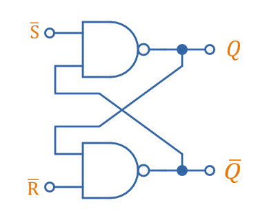
SR Latches
The SR (Set-Reset) latch is the most basic form of latch. It can be built from two cross-coupled NOR gates as shown below:

Driving either S or R high allows you to set the latch into the 1 or 0 state respectively. The state of the latch is represented by the output and its complement . Because of feedback from the outputs, driving both S and R low makes the latch “remember” or “retain” its last known state (holding). Below is the characteristic table for a SR latch built from NOR gates:
| S | R | Action | ||
|---|---|---|---|---|
| 0 | 0 | No change | ||
| 0 | 1 | 0 | 1 | Reset |
| 1 | 0 | 1 | 0 | Set |
| 1 | 1 | 0 | 0 | Not allowed |
Driving both set and reset high is a forbidden state, as it makes both and equal 0.
A SR latch can also be made with two NAND gates instead of two NOR gates:
When making the SR latch from NAND gates the invalid state is now and the hold state is , they switch positions compared to the SR latch built from NOR gates. This is also the reason why and have been renamed to and . Below is the full truth table:
| Action | ||||
|---|---|---|---|---|
| 0 | 0 | 1 | 1 | Not allowed |
| 0 | 1 | 1 | 0 | Set |
| 1 | 0 | 0 | 1 | Reset |
| 1 | 1 | No change |
You can play with the interactive NAND-gate based SR latch below:
SN74LS279 is a quad SR latch component by Texas Instruments. Two of the four latches have two set inputs, allowing for either to be active to set the latch (equivalent to an OR gate placed before a normal single set input SR latch).
SR latches can be used to make a switch debounce circuit.
Why Have Q And Q Bar?
You might wonder what the purpose of is, given it’s always the opposite of and you generally think of the value of representing the state of the latch. It’s because sometimes you do need the inverse of in further logic, and so providing it saves an inverter. And it’s needed in the internal logic of the latch anyway, so it’s not of great cost to provide a pin for it on the package.
How Does An SR Latch Work?
- is
HIGHand isLOW: Since is high, the output of the top NOR gate isLOW. ThisLOWfeeds into the bottom NOR gate, along with which is alsoLOW, thus the output of the bottom NOR gate isHIGH. ThisHIGHfeeds into the top NOR gate, which will keep the circuit in this defined state, even if is then brought LOW. This gives the SR latch its memory. - is
LOWand isHIGH: Because of the symmetry, the same things happens, but in reverse. isHIGHand isLOW. Again, if goes low, the SR latch “remembers” and keeps its outputs in the same state.

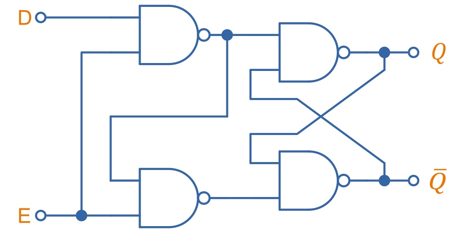
D Latch
A D Latch is like a SR latch except extra circuitry is added so that instead of a set and reset input, you obtain a single input to set or reset (), and an enable line (). This is generally a more practical type of latch as it can store the arbitrary state of a single line when told to do so by the enable input.
As the below diagram shows, a D latch is essentially a SR latch but with extra NAND gates and an inverter added to the front. The NAND gates “gate” the data line by anding it with the enable, such that when the enable line is 0, no signal gets through. The inverter acts to remove the need to separate “set” and “reset” lines of a traditional SR latch by providing the two signals from one input.
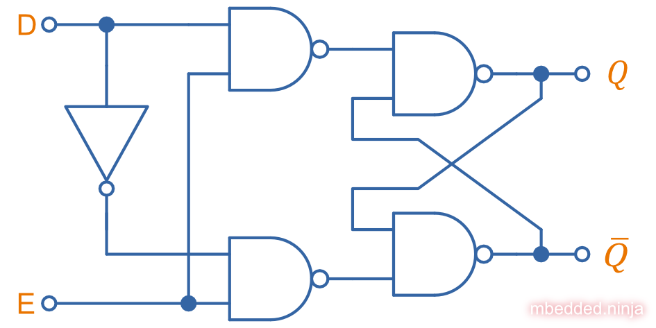
You can see from the below truth table that when , the latch remembers its last state. When , the signal on is passed onto the output:
| E | D | Action | ||
|---|---|---|---|---|
| 0 | 0 | No change | ||
| 0 | 1 | No change | ||
| 1 | 0 | 0 | 1 | Reset |
| 1 | 1 | 1 | 0 | Set |
You can actually simplify the above circuit and remove the need for an inverter altogether. Just realise the output of the top left NAND gate is always the inverse of D as long as E is high, so you can actually take the output of this as the inverted D and feed it into the bottom left NAND gate as shown:
The above design, when built using CMOS technology would require 16 MOSFETs (4 for each NAND gate).
You can also make a D latch with inverters and transmission gates. This will result in a lower total transistor count to implement than the NAND gate style D latch above. The below schematic shows one way of doing it:
The NAND gate implementation required 16 MOSFETs, but the above circuit only requires 12 (2 for each inverter, 2 for each transmission gate, and 2 to invert the enable signal to drive the transmission gates).
When is HIGH, the lower transmission gate is ON and the input is passed through to the output via two inverters. When is LOW, the higher transmission gate is ON and the output is fed back to itself via two inverters (hence performing the latching action). The Texas Instruments CD4042B uses a similar technique to implement its D latches1.
JK Latch
A JK latch is also known as the gated or clocked SR latch2. It is a level-triggered device, even though many online tutorials suggest it is edge-triggered. Along with this, many references call this a JK flip-flop. Based on the rules we decided on above (latches for asynchronous or level-triggered devices, flip-flops for edge-triggered devices), we are calling this a latch. The schematic symbol is:
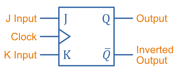
The letters J and K were chosen by the inventor of the JK latch, Jack Kilby3. A JK latch can be built with NAND gates with the following circuit:
Flip-Flops
Flip-flops are like latches, except their inputs are designed to be accompanied by a clock signal, and they only change their outputs at clock edges (according to our naming rules we decided upon). Flip-flops typically require more circuitry to achieve the edge-triggered behaviour, but offer more versatility.
In popular literature, some level-triggered devices are commonly called flip-flops, especially the “JK flip-flop”.
Edge Detection
The key feature about flip-flops is that they are edge-triggered rather than level-triggered. So how do you design a flip-flop to only do something on the edges of the clock signal? One very simple way is a circuit made from an inverter and an AND gate, and exploits the non-zero propagation delay time through the inverter. When the input changes from a 0 to a 1, the delay through the inverter causes both of the inputs to go high for a brief amount of time, which makes the output 1. This enables the latch for a very brief amount of time during the positive edge transition.
This is the basic schematic:

And this is what the timing looks like:
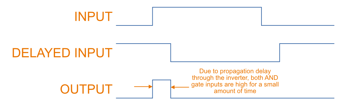
The problem with the above edge-detection circuit is that it cannot guarantee that the created pulse is long enough for the latch logic to obtain the correct state4. There are better ways to create edge-triggered flip-flops, which we will show when we introduce the master-slave D-type flip-flop below.
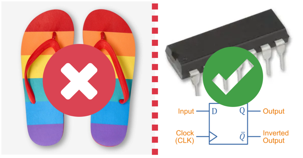
D-Type Flip-Flops
A D-type flip-flop (where the D either stands for Delay or Data depending on who you ask) is a flip-flop which is based off the D latch, with additional circuitry to make it edge-triggered instead of level triggered. Below are the basic symbols for a D-type flip-flop:
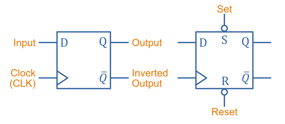
D-type flip-flops are used for counters, shift-registers and input synchronization.
D-Type Flip-Flops with Inverters
But how is a D flip-flop actually made? Basically, you could add the edge-trigger circuit to the (enable) line of a D latch (as shown above) to make a D flip-flop:
We now instead call the line the , to signify it is edge-triggered rather than level-triggered.
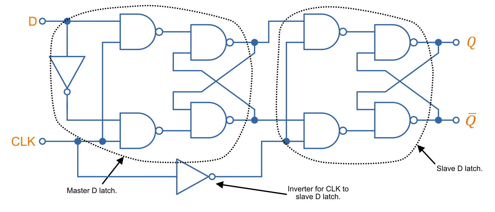
Master-Slave D Flip-Flop
Master-slave flip-flops are a another way of creating edge-triggered flip-flops from either level-triggered latches or flip-flops. Master-slave flip-flops are normally made from either two D flip-flops in series or two JK latches in series. The master is fed the raw clock signal (so is active while the clock is HIGH) whilst the slave is fed an inverted clock signal (and is active when the clock is LOW). Thus the master latch responds to the input while the clock is HIGH, and the slave is opaque. At the falling-edge of the clock, the master becomes opaque and slave becomes transparent, the master’s output is passed through the slave and onto the final output. This forms a negative edge-triggered flip-flop. The clock signal can be easily inverted to make a positive edge-triggered device.
A master-slave D flip-flop is made from connecting two D latches in series.
Below is an interactive simulation of negative edge-triggered master-slave D flip-flop. Click on the H (just below the D) to toggle the level of the data line, and watch the output change on the negative edge of the clock!
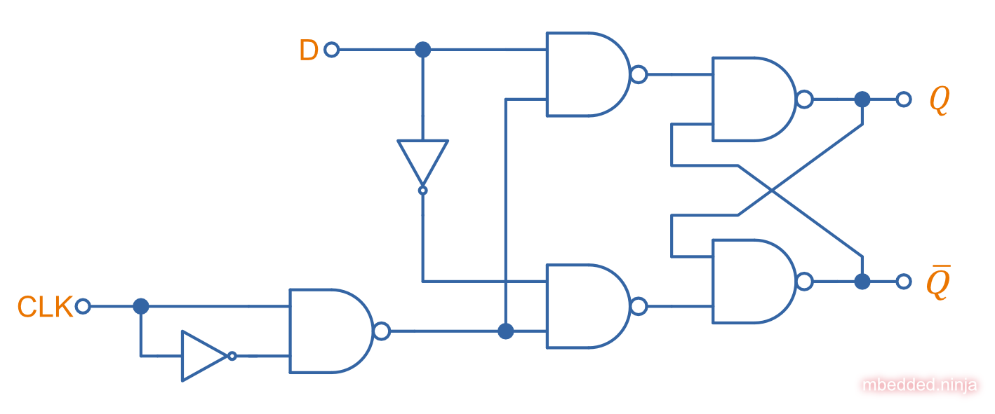
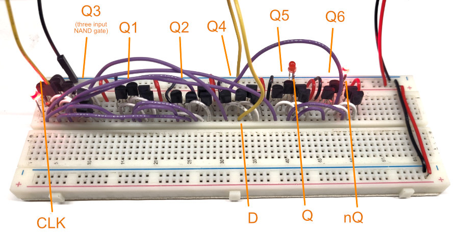
D-Type Flip-Flops with More NANDs
The above D-type master-slave flip-flop topology gives us reliable clock edge-triggered behaviour, but uses quite a few components (8 NAND gates + 2 inverters)! We can actually produce a functionality equivalent design with less components, with a clever arrangement of 6 NAND gates (of which 1 is 3-input, the rest 2-input). The logic diagram is:
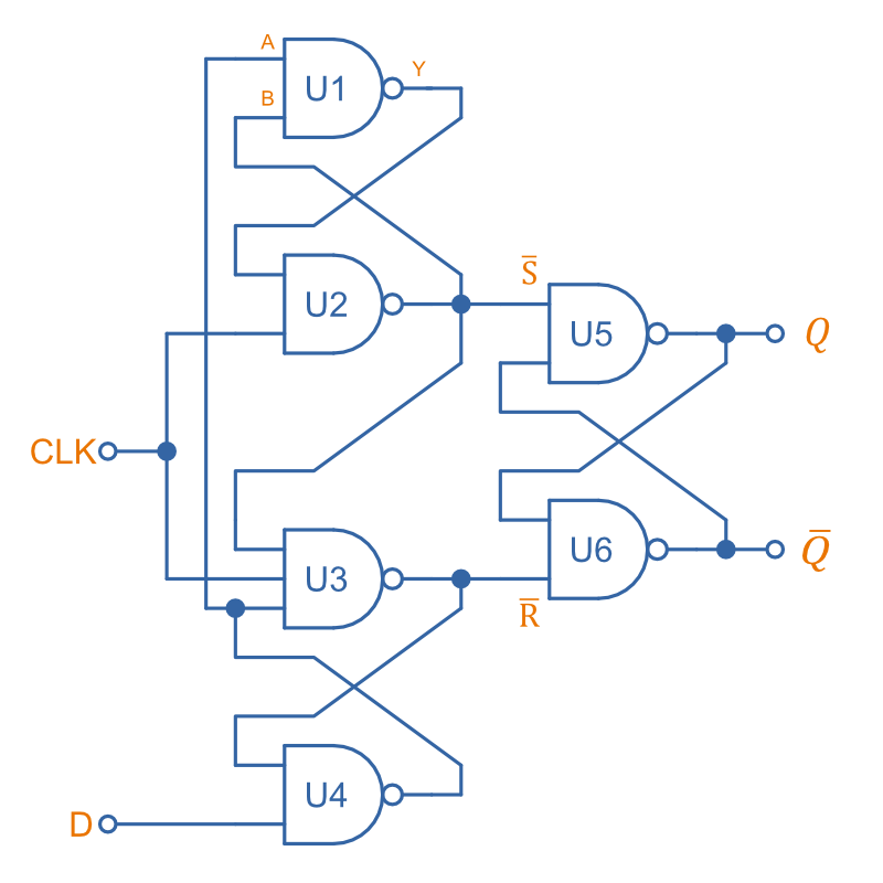
Roughly speaking, the above circuit is made from three SR latches, the output latch (center right), the input reset latch (upper left) and input set latch (lower left). Note that one of the input NAND gates has three inputs rather than two.
Let’s try and understand how this circuit works! To do so, we’ll assume you know how the output SR latch works (if you don’t, read the first part of this page!). This removes U5 and U6 from the analysis, we can just treat their inputs as the standard R and S (as annotated on the diagram). Now let’s walk through two scenarios, the first when the CLK transitions from 0 to 1 while D=0, and then second scenario the same clock transition when D=1. We’ll see what happens to the circuit if further changes to D are made once the transition finishes (HINT: nothing happens!).
What if D=0 when CLK transitions from 0 to 1?
- Before the transition,
D=0andCLK=0. Then at least 1 input to U2 and U3 is0. This means thatU2YandU3Ymust both be1. - Since
D=0andU3Y=1, thenU4Y=1. - Since
U4Y=1andU2Y=1, thenU1Y=0. This gives the following state for all inputs/outputs:Gate A B C Y U1 1 1 0 U2 0 0 1 U3 1 0 1 1 U4 1 0 1 - Now,
CLKtransitions to1.U2BandU3Bimmediately go high. - Within 1 propagation period,
U2andU3respond.U2doesn’t do anything becauseU2still has at least 1 of its inputs as0(U2A).U3however now has all three of its inputs high, and soU3Y=0. This gives the following state for all inputs/outputs:Gate A B C Y U1 1 1 0 U2 0 1 1 U3 1 1 1 0 U4 0 0 1 - If
Dnow changes from0to1while theCLKis high, it will have no effect as it’s blocked atU4by the factU4Ais now0.
What if D=1 when CLK transitions from 0 to 1?
- If
D=1,CLK=0then at least 1 input to U2 and U3 is0. This means thatU2YandU3Ymust both be1. - Since
D=1andU3Y = 1, thenU4Y=0. - Since
U4Y=0andU2Y=1, thenU1Y=1. - The rest of the gate inputs/outputs are easy to deduce.
- This gives the following state for all inputs/outputs:
Gate A B C Y U1 0 1 1 U2 1 0 1 U3 1 0 0 1 U4 1 1 0 - Thus,
R=1andS=1, and so the output latch is in a hold state. - Now
CLKimmediately transitions to1. Within 1 propagation delay, U2 and U3 respond.U2already hadU2A=1, and nowCLK=1makesU2B=1. This causes the gate to change state andU2Ygoes from1to0.U3doesn’t do anything however, as whileU3Bgoes to1,U3Cis still0, and so “blocks”U3from changing. This gives the following state for all inputs/outputs:Gate A B C Y U1 0 0 1 U2 1 1 0 U3 0 1 0 1 U4 1 1 0 - Thus
R=0andS=1, and the output latch gets “set”. - If
Dchanges back from1to0it will affect the output ofU4Ywhich will go from0to1. However, this output will not affect gatesU1andU3as they are both now “blocked” from changing becauseU2Y=0, meaning they both have at least one0input.
In Summary
When the CLK transitions from 0 to 1, the output latch gets set if D=1 and gets reset if D=0. Within 1 NAND gate propagation delay, further changes to D do not affect the output as D is now blocked by other 0’s and the inputs to the NAND gates (either immediately by U4 or by U2 and U3). This is the exact behaviour we wanted!
A common example of this style is the Texas Instruments SN7474 “Dual D-Type Positive-Edge Triggered Flip-flops with Preset and Clear”5.
This circuit gets even more complicated when you add asynchronous set and reset inputs! Rather than just the 1 three-input NAND gate, all NAND gates need to be three-input.
You can play around with the interactive D flip-flop simulation below. Toggle the level of the data line by clicking on the H, and watch the output only change on the positive edge of the clock!
D-Type Flip-Flops with Transmission Gates
In reality, the actual D-type flip-flops you can buy can be much more complicated than what we have just discussed! This is the logic diagram for the Nexperia 74HC74 dual D-type flip-flop IC6:
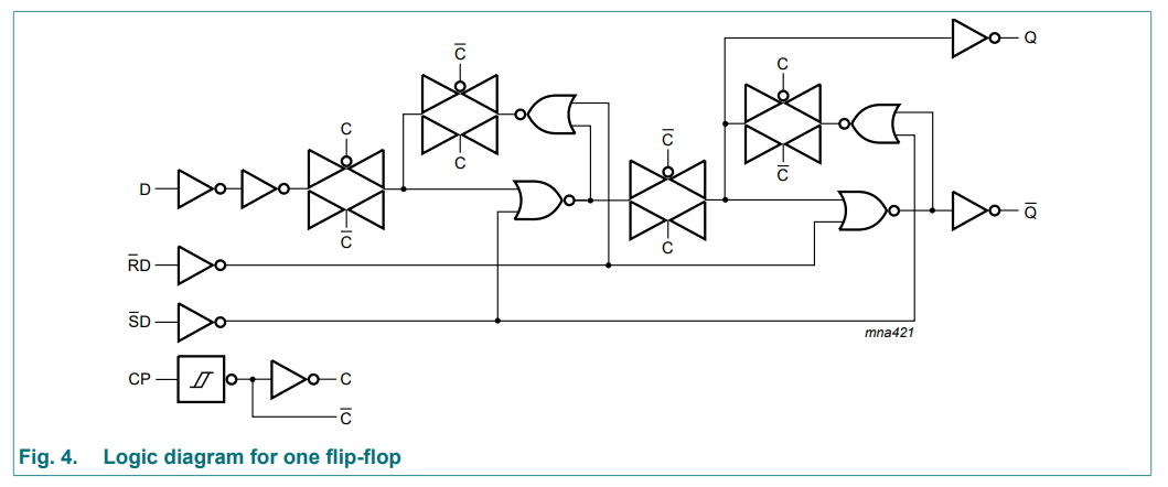
The four triangles pointing towards each other are transmission gates (TGs), normally made from one N-channel and one P-channel MOSFET connected in parallel (with the substrate not connected to the body, to avoid conduction through its internal diodes). Some of the circuitry that seems to serve no purpose (like the two inverters in series on the D input) has been presumably added to balance propagation times.
Examples
The partial part number 74HC74 is a dual D-type CMOS positive-edge triggered flip-flop with set and reset. It has balanced propagation delays. Orderable variants include the Nexperia 74HC74D and Toshiba 74HC74D.
Going from the 74 above to the 174 gives you a Hex (6 units) D-type flip-flop IC with reset. It has a shared CLK and reset line. One such example is the Texas Instruments CD74HC174.
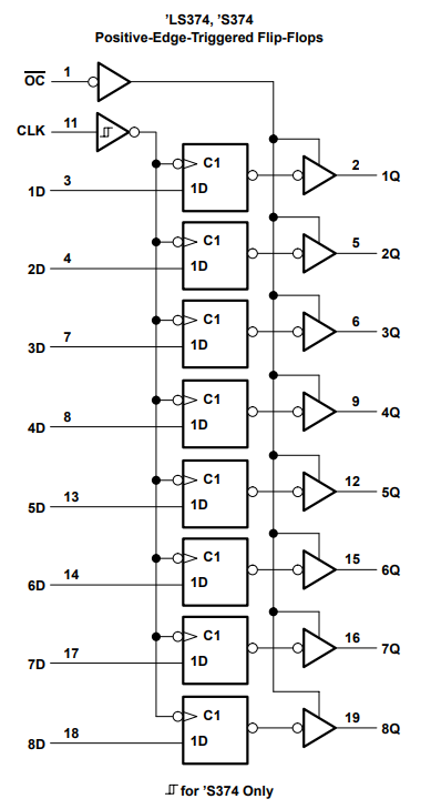
The partial part number LS374 is used for an 8-channel (octal) edge-triggered D-type flip-flop IC. The Texas Instruments 74LS374 is one such example.
Triggering
Edge-triggered D flip-flops can be either positive or negative edge triggered. Edge-triggered flip-flops are shown by a triangle at the clock input, and negative edge-triggered ones have an additional bubble. However, positive-edge triggered is much more common, and standard practice is to make a negative edge triggered flip-flop by adding your own inverting gate on the clock signal.
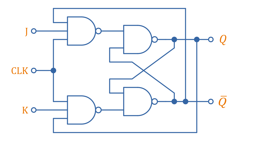
Master-Slave JK Flip-Flop
In a similar manner to the master-slave D flip-flop above, a master-slave JK flip-flop is made from connecting two JK latches in series. Sometimes the “master-slave” part of its name is dropped and this circuit is just called the JK flip-flop.
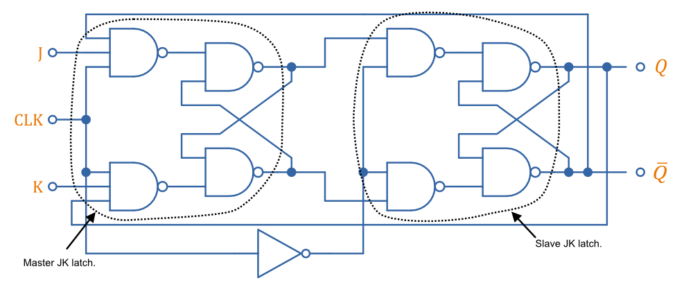
It behaves in the same manner as a JK latch, but only acts on the negative clock-edge. Here is the truth table for this NAND-gate based master-slave JK flipflop:
| Inputs | Outputs | Action | |||
|---|---|---|---|---|---|
| CLK | J | K | |||
| ↓ | 0 | 0 | No change | ||
| ↓ | 0 | 1 | 0 | 1 | Reset |
| ↓ | 1 | 0 | 1 | 0 | Set |
| ↓ | 1 | 1 | Toggle | ||
↓ represents the falling edge of the clock. All states for the clock except for the negative-edge (e.g. rising edge, high level, low level) do not cause any change.
You can play around with the interactive simulation below:
Timing Requirements
Setup and Hold Times
Synchronous flip-flops have timing requirements that must be obeyed. The two main requirements are:
- Setup time : This is the time that the data line must be stable for BEFORE the edge of the clock signal.
- Hold time : This is the time that the data line must be stable for AFTER the edge of the clock signal.
The below diagram shows this concept, assuming the logic is triggered on the positive-edge of the clock signal.
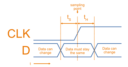
The edges of the signals have been drawn at a diagonal to illustrate that the signals do not instantly change state, and that the setup and hold times are defined from when the signal voltage passes through the half-way point between LOW and HIGH. In reality, the edges may not be straight lines but feature somewhat of an exponential curve due to capacitance.
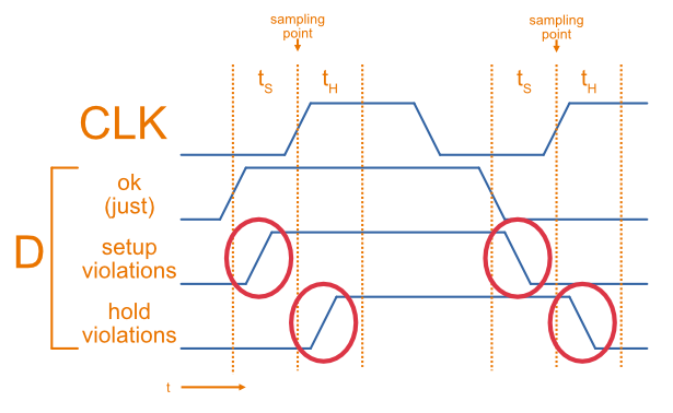
What do violating signals look like? Violating signals is when the data signal changes state in the setup or hold period, as illustrated in the diagram below.
Recovery and Removal Times
A similar but different concept to setup and hold times are recovery and removal times. Recovery and removal times are terms used to describe the timing requirements for edge-triggered logic for when asynchronous inputs (like set and reset) are de-asserted and the next clock edge8.
When set or reset are ASSERTED, there are no timing requirements since the action is asynchronous. The output of the flip-flop will get set or reset independent of the clock. However, when the set or reset is DE-ASSERTED, it’s not until the next clock edge that the flip-flop removes itself from the effects of set/reset and its output begins to follow again. This is where the recovery and removal time requirements come into play:
- Recovery time: The amount of time that the set/clear must stay de-asserted for BEFORE the clock edge.
- Removal time: The amount of time that the set/clear must stay de-asserted for AFTER the clock edge.
If both of these requirements are met, the flip-flop is guaranteed to come out of set or reset on that clock edge. If not, the flip-flop may encounter metastability.
Metastability
Metastability is the problem when digital logic persists for some unbounded amount of time in an invalid state. Metastability can cause glitches, the entirely wrong state, or invalid logic levels to propagate through digital logic systems.
Metastability can arise whenever a signal is sampled close to a transition, leading to indecision as to its correct value. — Montek Singh (UNC Chapel Hill) and Luciano Lavagno (Politecnico di Torino)9.
Metastability can occur under the following conditions:
- Digital circuits like edge-triggered D-type flip-flops require the input to be stable for some period before the clock edge (setup time) and some time after the clock edge (hold time) before it is allowed to change. If the input violates these timing conditions the flip-flop may encounter metastability.
- Asynchronous inputs arriving into a synchronous system. In this situation, you cannot totally eliminate the chance of metastability. The best you can do is to add synchronizers to the inputs to make the probability of metastability acceptably small10.
- When transferring data between two or more different clock domains (groups of circuitry running off different clocks).
Another key principle is that metastability occurs for an unbounded amount of time. That’s another way of saying there is no known upper limit to how long the metastability will take to resolve itself. You might think that this is very bad for any type of circuit. The good news is that the probability of the metastability occurring for longer and longer period falls with an exponential decay10.
Circuits Built From Latches And Flip-Flops
Toggle Flip-Flop
A toggle flip-flop can be made from an edge-triggered D-type flip-flop with its nQ connected to its D. The input signal is fed to the CLK.
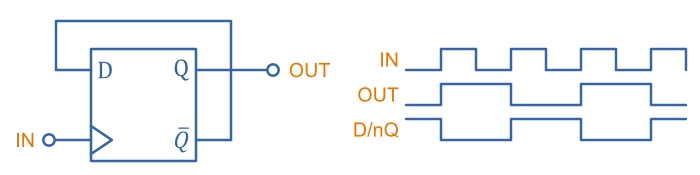
As you can see from the above timing diagram, the output toggles between high and low on every positive clock edge. This also can be considered a divide-by-two device (i.e. the output signal is half the frequency of the input), and is the basis for many digital counters11. Many of these could be connected in series, with the output of the first (Q) being connected to the input of the second (CLK). This would form a simple n-bit digital counter where n is the number of flip-flops in series.
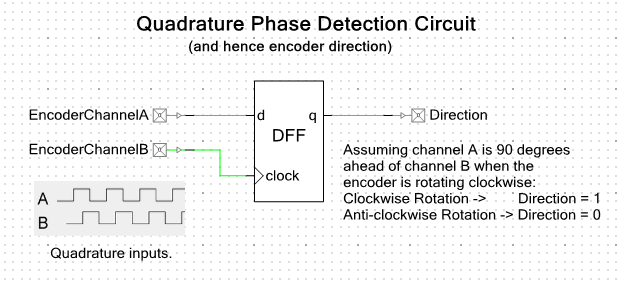
Quadrature Detection Circuit
This quadrature detection circuit is built entirely in hardware, and only uses one flip-flop. It is useful for detecting the direction that an encoder that outputs quadrature signals is spinning in. Potential applications include BLDC motor control. This circuit can be built entirely in reconfigurable PSoC on-chip logic.
When the encoder is spinning in one direction, the output will be logic high (1), when it is spinning in the opposite direction, it will be logic low (0).
Delay Circuit
A simple delay circuit can be made just by chaining DQ flip-flops together in series (the output of one feeds the input of another). For every flip-flop, the signal will be delayed by one clock-cycle (assuming they all share the same clock source).
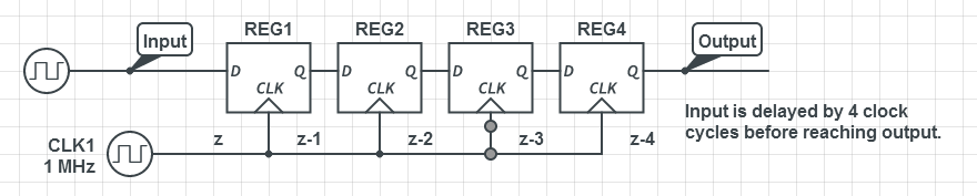
This can be used to make a simple timer. Obviously, a limitation is that a flip-flop is needed for every clock cycle of delay needed (try that with a 1000 clock cycle delay!). More advanced timers use binary encoding with the flip-flops to achieve a greater number of states for a lower number of flip-flops.
Footnotes
-
Texas Instruments (2003, Oct). CD4042B Types: CMOS Quad Clocked “D” Latch. Retrieved 2023-04-22, from https://www.ti.com/lit/ds/symlink/cd4042b.pdf. ↩
-
Priyanshu Vaish (2022, Aug 26). SR Flip-Flop: What is SR Flip-Flop Truth Table?. Byju’s Exam Prep. Retrieved 2023-04-14, from https://byjusexamprep.com/sr-flip-flop-truth-table-i. ↩
-
Electronics Tutorials. The JK Flip Flop. Retrieved 2023-04-14, from https://www.electronics-tutorials.ws/sequential/seq_2.html. ↩
-
Charles W. Kann (2021, May 28). Book: Digital Circuit Projects - An Overview of Digital Circuits Through Implementing Integrated Circuits (Kahn). 9.4: Edge Triggered Flip-Flop. LibreTexts: Engineering. Retrieved 2023-04-11, from https://eng.libretexts.org/Bookshelves/Electrical_Engineering/Electronics/Book%3A_Digital_Circuit_Projects_-_An_Overview_of_Digital_Circuits_Through_Implementing_Integrated_Circuits_(Kahn)/09%3A_Memory_Basics_-_Flip-Flops_and_Latches/9.04%3A_Edge_Triggered_Flip-Flop#:~:text=It%20is%20said%20to%20trigger,will%20be%20positive%20edge%20trigger. ↩
-
Texas Instruments (1988, March). SN5474, SN54LS74A, SN54S74, SN7474, SN74LS74A, SN74S74 - Dual D-Type Positive-Edge Triggered Flip-Flops With Preset And Clear. Retrieved 2023-04-12, from https://www.ti.com/lit/ds/symlink/sn54ls74a-sp.pdf. ↩ ↩2
-
Nexperia (2023, Feb 9). 74HC74; 74HCT74 - Dual D-type flip-flop with set and reset; positive edge-trigger. Retrieved 2023-04-11, from https://assets.nexperia.com/documents/data-sheet/74HC_HCT74.pdf. ↩ ↩2
-
Texas Instruments (2002, Aug). SN54LS373, SN54LS374, SN54S373, SN54S374, SN74LS373, SN74LS374, SN74S373, SN74S374 Octal D-type Transparent Latches and Edge-triggered Flip-flops. Retrieved 2023-04-12, from https://www.ti.com/lit/ds/symlink/sn54ls373-sp.pdf. ↩
-
VLSI Universe. Recovery and removal checks. Retrieved 2023-04-24, from https://vlsiuniverse.blogspot.com/2017/04/recovery-and-removal-checks.html. ↩
-
Ran Ginosar (2011, Oct). Metastability and Synchronizers: A Tutorial. IEEE CS/CASS. Retrieved 2023-04-23, from https://webee.technion.ac.il/~ran/papers/Metastability-and-Synchronizers.IEEEDToct2011.pdf. ↩
-
Wikipedia (2022, Nov 2). Metastability (electronics). Retrieved 2023-04-23, from https://en.wikipedia.org/wiki/Metastability_(electronics). ↩ ↩2
-
Eric Coates (2020, 29th Dec). Module 5.3: D Type Flip-flops. Learn about electronics. Retrieved 2023-04-18, from https://learnabout-electronics.org/Digital/dig53.php. ↩