Flash Memory

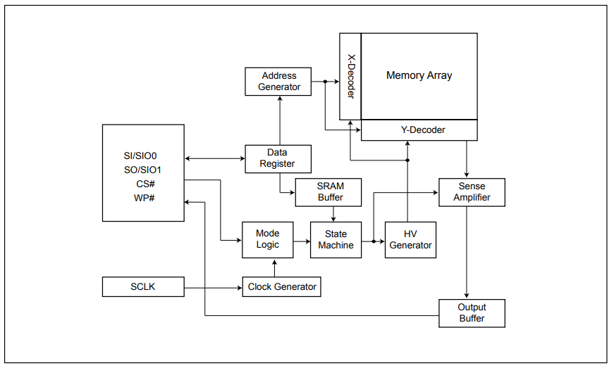
Flash ICs typically use the SPI communication protocol for communication to the MCU. This includes single lane SPI for slower flash and quad lane (QSPI) for faster flash. Data clock speeds of 80-100MHz are common1.
NOR Flash
Erase times can vary from approx. 50ms per 4KB sector to over 1s for the full chip1.
NAND Flash
Emulated EEPROM
You can use flash to store small bits of configuration data just like you can with EEPROM, but you must take care in how you read and write to it. To begin with, it pays to understand the differences between EEPROM and flash memory and why special measures are needed.
EEPROM is non-volatile memory that allows you to read and write single bytes of data, which can be useful in embedded applications for storing small amounts of configuration data (typically from 1 to a few kB’s in size). However, flash memory is designed with higher densities in mind and you cannot read and write at the byte level. To write to flash, you first have to erase an entire block (e.g. 4KB) and then write the entire block back.
Furthermore, flash memory has a much more limited number of write cycles compared to EEPROM. Flash endurance is typically in the 10,000-100,000 write cycles range, far less than EEPROM which is in the millions2.
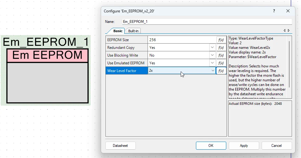
Firmware can be written to get around these flash limitations and provide the application with the same read/write a byte functionality that you get natively with EEPROM. This is called emulated EEPROM.
Writing an emulated EEPROM driver is a non-trivial task and requires careful consideration of the following:
- Wear levelling: To ensure that the same flash block isn’t written to over and over again, which would wear it out quickly.
- Error checking and correction: To ensure that the data read back is the same as the data written.
- Interrupted write error handling: To ensure that the system can recover from a failed write. A failed write may occur if the power is lost during a write operation. Remembering that you have to erase an entire sector, you must also be able to backup an entire sector.
- Wear indication: To provide feedback to the user on the health of the flash memory.
Some embedded firmware platforms have pre-built emulated EEPROM libraries. For example, PSoC Creator has an emulated EEPROM component that can be added to PSoC MCU based designs.
Footnotes
-
Macronix International Co. (2020, Sep 3). MX25V5126F - 2.3V-3.6V, 512K-BIT [x 1/x 2] CMOS Serial NOR Flash [datasheet]. Retrieved 2024-02-08, from https://www.macronix.com/Lists/Datasheet/Attachments/8750/MX25V5126F,%202.5V,%20512Kb,%20v1.1.pdf. ↩ ↩2 ↩3
-
Texas Instruments (2023, Apr). SLAAE58 - Application Note - EEPROM Emulation Type A Design. Retrieved 2024-09-18, from https://www.ti.com/lit/an/slaae58/slaae58.pdf. ↩