QFN Component Package

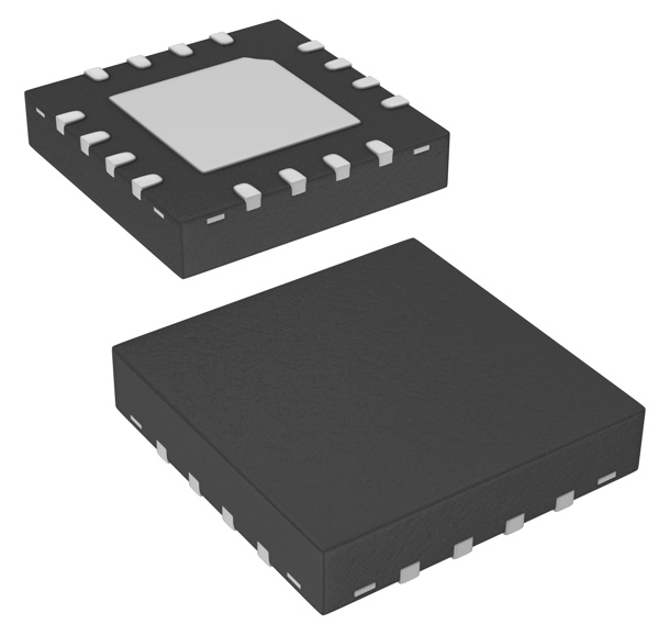
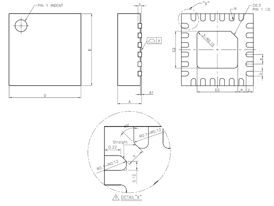
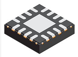
QFN is a family of SMD component packages with typically 12-108 leads. The QFN package is commonly used today for higher lead count ICs such as microcontrollers. It is a near chip-scale package, with all the pins being around the perimeter and an optional thermal pad in the centre. It is one of the highest pin-density SMD packages without resorting to BGA. Note that there are different pitch footprints within the QFN family! And QFN packages do not have to be square (square is the most common), some rectangular versions exist with a different number of leads on the two sides (opposite sides always have the same number of pins). The image below shows a typical QFN package with an equal number of leads on all sides and an exposed pad.
QFN packages offer benefits over other packages for high-speed circuits, as well as high heat dissipation capabilities. QFN packages lack gull-wing leads (like those present on the QFP package), which create noise in high-speed applications. However because the package is sitting right on the surface of the PCB (or very close to it), they suffer more from mechanical/thermal stress than other SMD packages with larger stand-offs, such as the QFP package.
Texas Instruments recommends rounded pads on the QFN package to prevent solder bridging. Also, stencil windows are recommended for the solder paste on the thermal pad so that a limited amount of solder is added. Too much solder can cause the QFN package to “float” around during the soldering process.
A QFN-like package with pins on only two of the four sides is a SON package (DFN).
Confusingly, NXP names its range of QFN packages with SOT… (e.g. SOT-762-1), a name which is commonly reserved for transistor packages such as the popular SOT-23.
Synonyms
2077-02: Freescale’s package code for a QFN-16, 5x3 pins, 3x3mm body package.CP-32-2: Analog Devices package code for a QFN-32, 8x8 pins, 0.50mm pitch, 5x5mm body package.HVQFN: NXP’s name for a heatsink very-thin QFN (i.e. a QFN with an exposed thermal pad). Some HVQFN outlines are also available with wettable flanks (denoted by a(DD)suffix on the outline drawing number).LFCSP: Analog Devices.MLF: Micro-leadframe.MLP: Fairchild Semiconductor.2QFN-UT: Samtech’s name for ultra-thin QFN packages.RSB: Texas Instruments’ drawing code for a QFN-40 package.RSN: Texas Instruments’ drawing code for a QFN-32, 8x8 pins, 4.15x4.15x0.80mm body, 0.40mm pitch package.3RQZ: Texas Instruments’ drawing code for a QFN-48, 7x7mm, 0.50mm pitch package.SOT-xxx: NXP’s name for its QFN range of packages; note this does not include packages such as the SOT-23, which are NOT QFN packages.SOT-762-1: NXP’s name for a QFN-14, 2.5x3.0mm, 0.5mm pitch EP package.4T3B: Microchip’s code for a VQFN-48, 7x7x0.9mm, 0.5mm pitch, 5.15x5.15mm EP package.5TMB: Microchip’s code for a VQFN-64, 9x9x0.9mm, 0.5mm pitch, 4.70x4.70mm EP package.5UFD: Linear Technology’s (now Analog Devices) code for a QFN-28, 5x4mm, 0.5mm pitch, 3.65x2.65mm EP.6ZLG: Atmel’s code for a VQFN-48, 7x7x0.9mm, 0.5mm pitch, 5.15x5.15mm EP package.5ZST: Atmel’s code for a VQFN-64, 9x9x0.9mm, 0.5mm pitch, 4.70x4.70mm EP package.5
Variants
- The following acronyms are used to describe a QFN package with a different package height:
- UQFN
- VQFN
- QFN packages come in different pitches (0.40, 0.45, 0.50, 0.65mm).
- QFN packages may or may not have a central exposed pad on the underside.
Dimensions
Common pitches:
- 0.40mm
- 0.45mm
- 0.50mm
- 0.65mm
Note that the max. height for almost any QFN package is 1mm (including stand-off). Some have a smaller height (e.g. the UT/ultra-thin QFN packages).
0.40mm pitch QFN package dimensions (LxWxH), with the land area (LA) in brackets:
- QFN-UT-20: 3x3x0.6mm (LA: 9mm²)
- QFN-56: 7x7x1mm (LA: 49mm²)
- QFN-64: 8x8x1mm (LA: 64mm²)
- QFN-72: 9x9x1mm (LA: 81mm²)
- QFN-88: 10x10x1mm (LA: 100mm²)
- QFN-108: 12x12x1mm (LA: 144mm²)
0.50mm pitch QFN package dimensions (LxWxH):
- QFN-16: 3x3x1mm (LA: 9mm²)
- QFN-20: 3x3x1mm (LA: 9mm²)
- QFN-24: 4x4x1mm (LA: 16mm²)
- QFN-32: 5x5x1mm (LA: 25mm²)
- QFN-36: 6x6x1mm (LA: 36mm²)
- QFN-48: 7x7x1mm (LA: 49mm²)
- QFN-56: 8x8x1mm (LA: 64mm²)
- QFN-64: 9x9x1mm (LA: 81mm²)
- QFN-68: 10x10x1mm (LA: 100mm²)
0.65mm pitch QFN package dimensions (LxWxH):
- QFN-16: 4x4x1mm (LA: 16mm²)
- QFN-20: 4x4x1mm (LA: 16mm²)
- QFN-32: 7x7x1mm (LA: 49mm²)
Solderability
Surprisingly easy to solder by hand, as long as the pads extend around to the sides of the IC, and you drill a hole to solder the centre pad from the reverse. QFN packages can also be soldered easily with an infrared rework station or the “frying pan” technique.
Solder Mask
TI recommends a non-solder mask defined (NSMD) pad over a solder mask defined (SMD) pad. This is to produce consistent and reliable solder joints. As a rule-of-thumb, you want solder mask openings that are 0.1-0.14mm larger than the pad size. By default, Altium uses NSMD pads.
Some QFN packages have an exposed metal feature on the underside to indicate pin 1. If this is the case, make sure this area is covered with solder mask to prevent shorting to neighbouring traces. This is an unusual feature, and personally I have not used any QFN packages with this present.
The Central Pad And Solder Paste
It is recommended to reduce the amount of solder paste applied to the centre pad (also called the mechanical pad or thermal pad) to prevent the QFN package from floating during reflow. A rule-of-thumb is to have 50-80% coverage on the centre pad (this obviously does not apply to QFN packages with no pad).
It may be necessary to mask or plug vias in the centre pad to prevent solder paste being carried through the via and away from the pad during reflow. Small-holed vias (such as vias with a hole diameter of 0.3mm or less) do not normally cause a big problem.
The central pad may not necessarily be electrically connected to anything.
Singulation Methods
There are two singulation methods for QFN packages:
- Punch singulation: This is used on individually-moulded QFN packages.
- Saw singulation: This is used on moulded array QFN packages.
The main difference between these two singulation methods is the cross-sectional profile. Punch singulation gives a tapered cross-section (larger cross-section at the bottom than the top), while saw singulation gives a completely square cross-section.
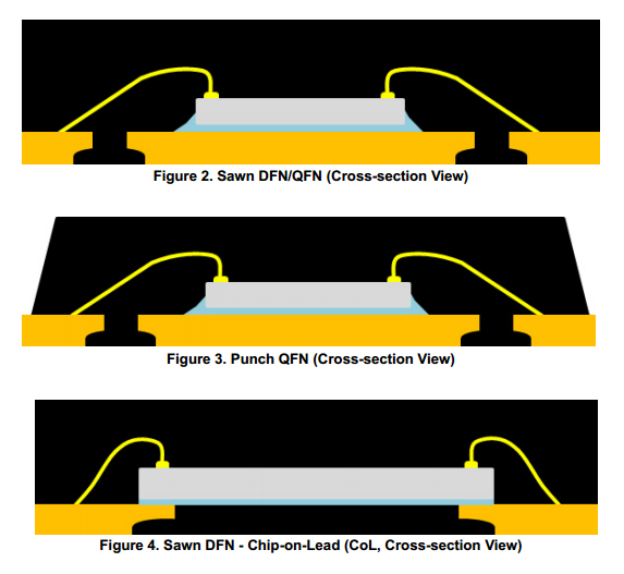
Punch singulated QFN packages are JEDEC compliant.
Voiding
Volatiles that get trapped underneath the pad during reflow can cause voids to form underneath the component (areas where the pad is not soldered to the PCB). Another potential cause of voiding is when too much solder paste is applied to the centre pad, which causes the package to float on the PCB during reflow.
Stresses
Because the QFN package sits directly on the PCB and has no standoff, they are less resilient to mechanical stresses than packages with leads such as QFP packages. The amount of PCB flex must be taken into consideration. Excessive stress can damage a QFN package.
Lead Styles
Unique Corner Pins
QFN packages exist where the corner pins have to be of a different shape to all the others for clearance reasons. The only example of this I have ever seen is the package for the InvenSense MPU-9250 IMU. It is a QFN package with 24 pins in a 3x3x1.0mm size with six 0.40mm pitch pins on each edge. Because of the high pin density, the outer pins on each edge almost touch each other, and so a different pin shape is used. This also means you use a different pad shape for the package footprint.
Completely Non-Standard QFN Packages
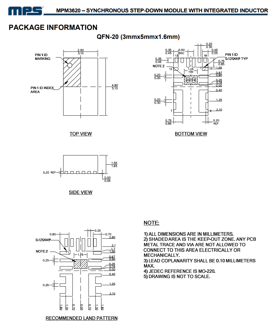
Aside from the unique corner pins that QFN packages can have (as explained above), some QFN packages are completely IC specific and do not follow the “standard” at all. One example is the MPM3620, which comes in a “QFN-20” component package with changing pitch, different sized pins, bridged pins and internal pins near the bottom centre of the package.8
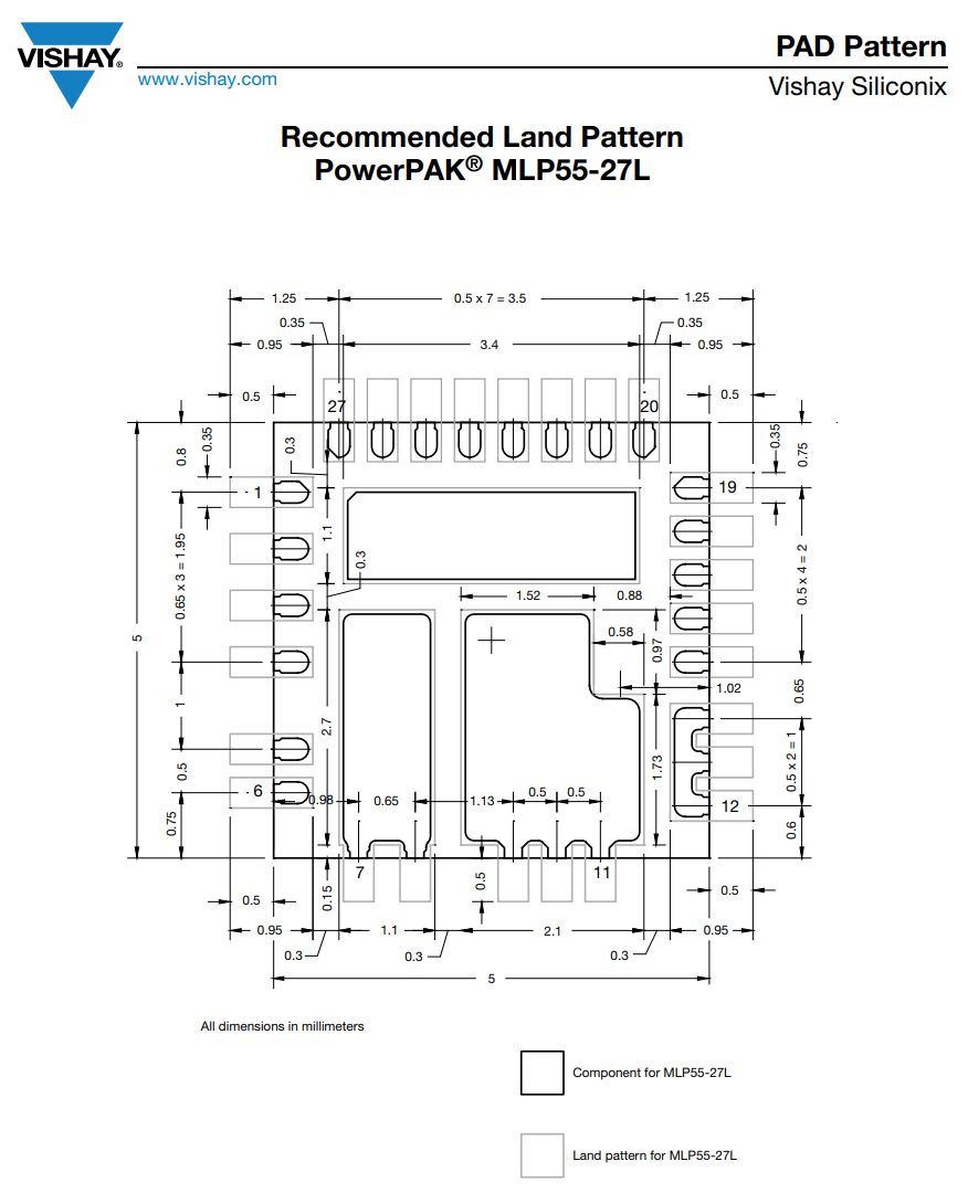
MLP is a common package name used for “non-standard” QFN-like packages, an example is shown below:
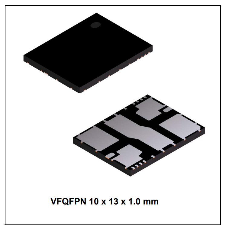
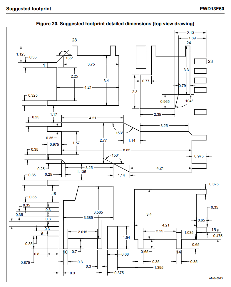
Another great example is STMicroelectronics’ PWD13F60 high-voltage full-bridge with integrated gate driver IC. It comes in a VFQFPN 10x13x1.0mm package which contains a variety of pad shapes and sizes, as shown in the below image:
Want to see the recommended footprint for this IC? See below!
Standardization Of Pinout For Logic Functions
JEDEC has a standard on the pinout of QFN packages for logic functions.
JESD75-5 - JEDEC Standard - QFN Pinouts For Logic Functions
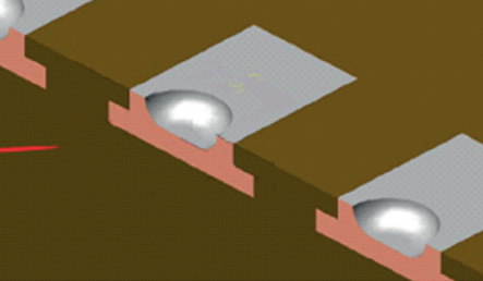
Wettable Flanks
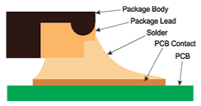
Component packages which have wettable flanks have a step-cut lead frame and tin added to the sidewalls of the package. This allows a side fillet of solder to form more reliably, aiding automatic optical inspection (AOI) (QFN packages already had pad metallization on the side of the package, but no step-cut nor plating, and side-fillet formation was less reliable).10
The QFN package is one of the most common packages for a manufacturer to add wettable flanks to. The wettable flanks feature was largely driven by the need for AOI in the automotive industry, but it is now found to be generally useful in a number of industries.
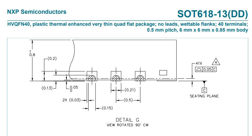
The tin plating of the flank prevents the traditionally exposed copper (a by-product of the sawing singulation of a single QFN package from a “brick”) from oxidizing.11
Thermal Resistances
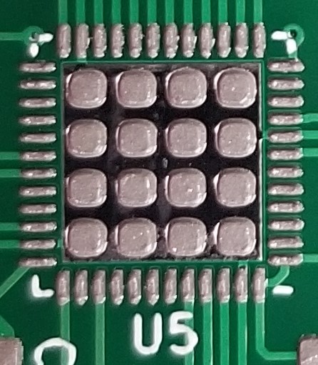
LFCSP-16
Similar To
- QFP: Similar to QFN except QFP has gull-wing leads that protrude from the body. For the same pin count, QFP is larger than QFN.
- SON (DFN)
Footnotes
-
DigiKey. ISL84467IRTZ-T - 4 Circuit IC Switch 2:1 400mOhm (Typ) 16-TQFN (3x3) [product page]. Retrieved 2023-08-02, from https://www.digikey.com/en/products/detail/renesas-electronics-america-inc/ISL84467IRTZ-T/1978117. ↩
-
Fairchild Semiconductor (2005, Sep). PCB Land Pattern Design and Surface Mount Guidelines for MLP Packages [application note]. Retrieved 2022-03-09, from http://educypedia.karadimov.info/library/AN-5067.pdf. ↩
-
Texas Instruments (2018, May). bq25703A - I2C Multi-Chemistry Battery Buck-Boost Charge Controller With System Power Monitor and Processor Hot Monitor [datasheet]. Retrieved 2023-08-02, from https://www.ti.com/lit/ds/symlink/bq25703a.pdf. ↩
-
NXP (2019, Aug 2). SOT762-1 - plastic, dual in-line compatible thermal enhanced very thin quad flat package; no leads; 14 terminals; 0.5 mm pitch; 2.5mm x 3 mm x 0.85 mm body [package outline drawing]. Retrieved 2024-04-29, from https://www.nxp.com/docs/en/package-information/SOT762-1.pdf. ↩
-
Microchip (2021). SAM D21/DA1 Family Low-Power, 32-bit Cortex-M0+ MCU with Advanced Analog and PWM [datasheet]. Retrieved 2022-03-02, from https://ww1.microchip.com/downloads/en/DeviceDoc/SAM-D21-DA1-Family-Data-Sheet-DS40001882H.pdf. ↩ ↩2 ↩3 ↩4
-
Linear Technology (now Analog Devices). LT3922-1 - 36V, 2.3A Synchronous Step-Up LED Driver with 25,000:1 PWM Dimming [datasheet]. Retrieved 2023-08-02, from https://nz.mouser.com/datasheet/2/609/lt3922_1-3123537.pdf. ↩
-
Freescale Semiconductor. AN1902: Quad Flat Pack No-Lead (QFN) [application note]. Retrieved 2026-07-06, from http://cache.freescale.com/files/analog/doc/app_note/AN1902.pdf. ↩
-
Monolithic Power Systems. MPM3620 - 24V Input, 2A Module Synchronous Step-down Converter with Integrated Inductor [datasheet]. Retrieved 2026-07-06, from https://www.monolithicpower.com/en/documentview/productdocument/index/version/2/document_type/Datasheet/lang/en/sku/MPM3620GQV/document_id/2092. ↩
-
STMicroelectronics (2017, Dec). PWD13F60: High-density power driver - high voltage full bridge with integrated gate driver [datasheet]. Retrieved 2022-04-19, from https://www.st.com/resource/en/datasheet/pwd13f60.pdf. ↩ ↩2
-
David Snook (2018, Jan 23). Make automatic optical inspection easy thanks to packages with wettable flanks [blog post]. Texas Instruments. Retrieved 2021-10-27, from https://e2e.ti.com/blogs_/b/behind_the_wheel/posts/make-automatic-optical-inspection-easy-thanks-to-packages-with-wettable-flanks. ↩
-
Bradley Smith (2017). Wettable Flank Plated PQFN [article]. Allegro MicroSystems. Retrieved 2021-10-27, from https://www.allegromicro.com/en/insights-and-innovations/technical-documents/semiconductor-packaging-publications/wettable-flank-plated-pqfn. ↩ ↩2 ↩3
-
NXP (2018). SOT618-13(DD) HVQFN40, plastic thermal enhanced very thin quad flat package; no leads, wettable flanks; 40 terminals; 0.5 mm pitch, 6 mm x 6 mm x 0.85 mm body [package outline drawing]. Retrieved 2021-10-28, from https://www.nxp.com/docs/en/package-information/SOT618-13(DD).pdf. ↩