Chip (EIA) Component Packages

Surface-mount resistors, MLCC capacitors and ferrite beads are commonly packaged in a set of standardised chip packages. These package sizes are standardised by both the IEC in metric units and the EIA in imperial units.
They are defined by four-digit number which represents the total footprint width and height, respectively (assuming the two footprint pads are on the left and right rather than the top or bottom, or more formally, the axis of the component runs parallel to the width).
In metric units, the format is to use two number each to describe the width and height in tenths of a millimeter, e.g. a chip package size ‘2012’ tells you the width is 2.0mm and the height is 1.2mm. In imperial, the numbers are in hundredths of an inch (which is NOT mills — that is thousandths of an inch). For example, an 0805 chip package tells you the width is 0.08inch, and the height 0.05inch. This is equivalent to the ‘2012’ metric representation. Below is a short description on the most popular chip packages. The imperial size of the footprint is listed first, and then the metric equivalent is followed in brackets.
The following is a list of the common chip packages, sorted from smallest to largest:
| Package Designator (metric, IEC) | Dimensions (metric) | Package Designator (imperial, EIA) | Dimensions (imperial) | Typical Power Rating (W) | Land Area | Comments |
|---|---|---|---|---|---|---|
| 0402 | 0.4x0.2mm | 01005 | 0.0157x0.0079in | 1/32 | Ridiculously small chip package that can barely be seen by the naked eye. | |
| 0603 | 0.6x0.3mm | 0201 | 0.024x0.012in | 1/20 | 0.12mm² | Small chip package that is unsolderable by hand (it is just too small). BE CAREFUL NOT TO GET THE METRIC SIZE CONFUSED AS AN IMPERIAL as an 0603 imperial also exists! |
| 1005 | 1.0x0.5mm | 0402 | 0.039x0.020in | 1/16 | 0.5mm² | These are too small for ‘legitimate’ hand soldering, but it can be done. A common size for resistors and small valued capacitors in the pico/nanofarad range. |
| 1608 | 1.6x0.8mm | 0603 | 0.063x0.031in | 1/16 | 1.28mm² | This package supports all resistors, and ceramic capacitors up to 10uF. My favourite package size! You can easily solder these with a little experience. You can route a small track between the pads (given a distance of 0.6mm between the inside edges of the two pads, this just allows for a 0.2mm track and 0.2mm gap on each side, which is a common minimum clearance rule). |
| 2012 | 2.0x1.25mm | 0805 | 0.079x0.049in | 1/10 | 2.4mm² | Supports ceramic capacitors up to 47uF. You can easily route a track between the two pads. |
| 2518 | 1007 | ? | 4.5mm² | Commonly used for chip inductors are the 100uH, 250mA mark. | ||
| 3216 | 3.2x1.6mm | 1206 | 0.126x0.063in | 1/8 | 5.1mm² | One of the larger forms of SMT resistor/cap packages. Many of the bigger valued ceramic capacitors (100uF and up), come in this package, as well as the higher wattage resistors. Although smaller than their through-hole equivalents, 1206 components still take up a considerable amount of space on a PCB. Very easy to hand solder though! |
| 3225 | 3.2x2.5mm | 1210 | 0.126x0.098in | 1/4 | 8.0mm² | Slightly fatter version of the 3216, and hence can handle more power. |
| 4516 | 4.5x1.6mm | 1806 | 0.177x0.063in | ? | 7.2mm² | |
| 4532 | 4.5x3.2mm | 1812 | 0.18x0.13in | 1/2 | 14.4mm² | |
| 5025 | 5.0x2.5mm | 2010 | 0.197x0.098in | 1/2 | 12.5mm² | |
| 6432 | 6.4x3.2mm | 2512 | 0.25x0.13in | 1 | 20.48mm² | One of the largest SMT chip packages you can get. Limited supply of components in this package, mainly power and current-sense resistors. |
7451 or (73511) | 7.4x5.1mm | 2920 | 0.29x0.20in | mm² | Used for PTC resettable fuses2. |
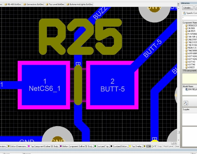
The following image shows how you can easily route an 0.2mm thick trace between the pads of a 0805 component.
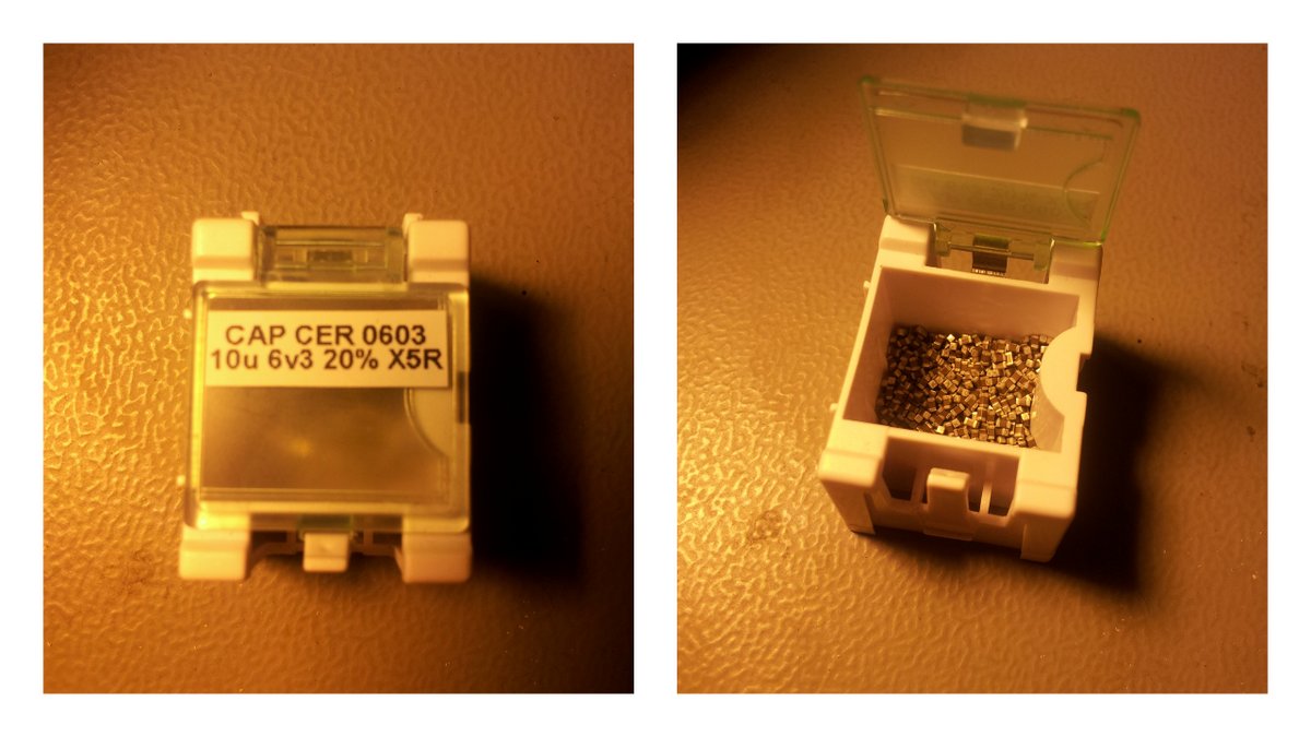
The following image is of 0603 (imperial) SMD components inside a small container.
SMD Chip Resistors
The following table shows the range of chip resistors package sizes (based on the EIAJ Chip Packages above), and typical parameters for each. Note that the maximum current rating is based on the thermal properties of the package and its leads, and does not take into account the actual resistance of the resistor (e.g. tested with a 0Ω resistance). Obviously, the actual allowable current is likely to be much less due to resistance.
| Designator (metric) | Designator (imperial, EIA) | Max. Current (A) |
|---|---|---|
| 1005 | 0402 | 1 |
| 1608 | 0603 | 1 |
| 2012 | 0805 | 2 |
| 3216 | 1206 | 2 |
| 3225 | 1210 | 3 |
| 5025 | 2010 | 3 |
| 6432 | 2512 | 3 |
Footprints
Every PCB CAD program worth it’s weight in salt will provide footprints for the standard chip packages in their default libraries.
There are reports that the default 0402 (imperial) footprint that is shipped with Eagle is non-ideal and causes “head-in-pillow” and/or tombstoning. See https://www.worthingtonassembly.com/perfect-0402-footprint for more details3.
Reverse Geometry Chip Capacitors (LICC)
Reverse geometry chip capacitors (named LICC (Low Inductance Chip Capacitor) by Kyocera AVX4) have their leads on the long sides of the chip, as opposed to standard chip components which have the leads on the short sides. This reverse geometry reduces the length of the current path through the component and reduces the parasitic inductance of the capacitor (less than 400pH5). For applications such as high-speed design, when capacitors are used for noise decoupling, the parasitic inductance needs to be as low as possible to increase the capacitors resonant frequency5.
They are normally named the same as normal chip capacitors except with the two numbers in reverse order, i.e. an 0603 sized capacitor now becomes a 0306 capacitor.
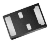
MEMS Oscillators
Some MEMS oscillators uses chip package sizes, but with extra pins for power and ground. One common package size is 2012 (2.0x1.2mm) which is sometimes used for 32.768kHz crystal oscillators (XTAL):
Footnotes
-
Mouser. 2920 (7351 metric) Resettable Fuses - PPTC Datasheets. Retrieved 2022-01-25, from https://www.mouser.com/c/ds/circuit-protection/thermistors/resettable-fuses-pptc/?package%20%2F%20case=2920%20%287351%20metric%29. ↩
-
Bel. 0ZCF Series. Retrieved 2022-01-25, from https://www.belfuse.com/product-detail/circuit-protection-0zcf-series. ↩
-
Worthington (2020). The Perfect 0402 Footprint. Retrieved 2023-06-14, from https://www.worthingtonassembly.com/perfect-0402-footprint. ↩
-
Kyocera AVX. Low Inductance Capacitors. Retrieved 2023-06-14, from https://datasheets.kyocera-avx.com/LICC.pdf. ↩
-
TDK. Reverse Geometry MLCC (C Series). Retrieved 2023-06-14, from https://www.tti.com/content/ttiinc/en/manufacturers/tdk/products/TDK-Reverse-Geometery-Multilayer-ceramic-capacitor-MLCC.html. ↩ ↩2
-
TDK (2022, Dec). Multilayer Ceramic Chip Capacitors - Commercial grade, low ESL reverse geometry (datasheet). Retrieved 2023-06-14, from https://product.tdk.com/en/system/files?file=dam/doc/product/capacitor/ceramic/mlcc/catalog/mlcc_commercial_lwreverse_en.pdf. ↩