Boost Converters

Boost converters (also called step-up converters) are a particular topology of switch-mode power supply (SMPS) that use a switching element, inductor, diode (or second switch) and capacitor to convert an input voltage into a higher (or equal) output voltage.
To learn more about EMI/EMC considerations regarding boost converters, see the EMC Design Guidelines page.
Schematics
Boost converters use a switching element, inductor, diode, and capacitor to convert an input voltage into a higher or equal output voltage .

How A Boost Converter Works
For an ideal boost converter (no component losses, operating in continuous conduction) the output voltage is determined purely by the input voltage and the duty cycle :
is the duty cycle (the fraction of each switching cycle the switch is on) and varies from to . Since , the output is always greater than or equal to the input — the converter can only step the voltage up.
The same “the average voltage across the inductor must be 0 over an entire switching cycle” argument used for the buck converter gives us this equation:
- When the switch is closed (), the inductor is connected directly across the input, so the voltage across it is . The inductor current ramps up, storing energy in its magnetic field.
- When the switch opens (), the inductor current can’t stop instantly, so it keeps flowing through the only path available: from the input, through the inductor and diode and into the output. To maintain this current, the inductor reverses its voltage polarity (its switch-node end swings above the input). The output voltage sits at approx. .
- Setting the average (integral) of the inductor voltage over the whole cycle to 0: using and therefore .
Design Procedure
Duty Cycle
The duty cycle for a boost converter is given by:1
As you can see, the duty cycle is dependent only on the ratio between the input and output voltages. This has to be one of the simplest boost converter equations. This equation ignores the specific voltage drops across the switching element and rectifier, but rather lumps them together into the efficiency term.
Inductance
The inductance can be determined using:
You don’t know or yet, but the trick is here to assume a maximum inductor ripple current as a percentage of the average inductor current, . A rule-of-thumb is to assume a maximum ripple current of 35% (assuming it is operating in CCM). Thus,
Now the equation for the inductance becomes:
which can be solved as we know all of the variables.
Output Capacitor
During the diode is reverse-biased and the load is supplied entirely by the output capacitor. This makes the capacitor’s job harder than in a buck converter — it sees a pulsed current rather than the inductor’s smooth triangular ripple, so both the RMS ripple current and the resulting output voltage ripple are larger.
The minimum output capacitance for a target output voltage ripple is:1
where:
is the output current
is the duty cycle
is the switching frequency
is the maximum desired output voltage ripple
As with the buck converter, the capacitor’s ESR adds further ripple on top of this. Because the boost output capacitor also carries significant RMS ripple current, check the capacitor’s ripple-current rating, not just its capacitance and voltage rating.
Output Current
The maximum output current is given by:
Diode Selection
The maximum reverse voltage of the diode must be at least equal to the output voltage of the boost converter. This is because the diode sees the full output voltage in reverse when the switch is closed.
Boost Converter Calculator
Use the generic boost-converter design helper below to compute the duty cycle, average and peak inductor current, and required inductance from the supply/output voltages, diode and switch drops, switching frequency, output current and acceptable inductor ripple.
PCB Routing
The same rules apply for routing boost converters as with any SMPS. See the PCB Routing section on the SMPS page for more information.
Light Load Instabilities
Bad things can happen when boost converters are operated with light/no load. If the controller isn’t smart enough to reduce the duty cycle down to near 0 when there is no or little load, the voltage across the capacitor can build up to a point where it causes damage to part of the circuitry.
Also, if the converter is in DCM and the load current suddenly increases, the output voltage can sag greatly.
Turning Off/Disabling
While most boost controllers have an enable/disable pin, this doesn’t actually disconnect the input from output, as the switching device is not in series with input and output, as it is in a buck converter. Thus if you need the load completely disconnected from the input, you will need to add something like a P-Channel MOSFET or load switch to the front-end of the boost converter.
Start-up vs. Runtime Minimum Input Voltage Requirements
Some boost converters have differing start-up and runtime minimum input voltage requirements. Typically, the boost converter requires a higher minimum input voltage to start (e.g. 18V), but once running, can run off a lower voltage (e.g. 500mV).
Bypass
Some boost converters designed for ultra-lower power applications have a bypass mode. When the output voltage is not needed to be higher than the input voltage, the converter enters a bypass mode in where most of the control circuitry is disabled, the converter stops switching, and the input voltage is “bypassed” straight to the output.
Max. Current Ratings
One gotcha: The “max. current” rating that a manufacturer will provide with a boost controller with an integrated switch will usually be the maximum current rating of the switch. This is not the maximum output current, but rather the maximum input current. The maximum output current, assuming you have a higher output voltage, will be less than this.
Compensation Loop
The compensation loop is part of the feedback mechanism.2 The below diagram shows a current-mode controlled boost converter with a transconductance amplifier () providing the feedback.
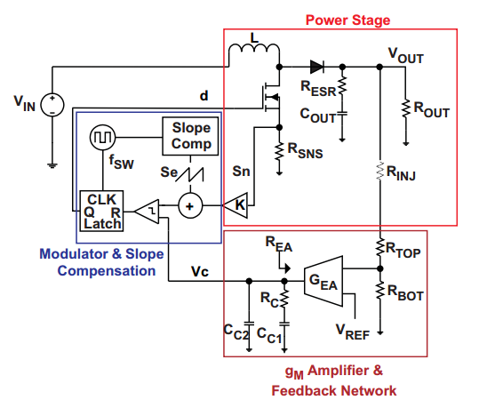
The above model is only valid for when the boost converter is acting like a current-mode controlled regulator. This is the case when the ripple current is within the normal operating region (0.2-0.4 times the average input current). When the inductor is oversized to further reduce current ripple through the inductor (less than 0.2 times the average input current), the boost converter behaves more like a voltage-mode controlled regulator and this above model is no longer valid.
External compensation can be added if the manufacturer provides a compensation pin (typically called COMP). The pin is the output of the internal transconductance amplifier.
A resistance between 5–100 kΩ and a capacitance between 1–10 nF is typical. A higher resistance corresponds to a faster response time. A lower capacitance corresponds to a higher phase margin.
Down Conversion
Some boost converters also have a built in regulator to provide regulation when the input voltage exceeds the desired output voltage. This is normally a linear regulator, so your efficiency will drop and you will have to take into account the thermal dissipation. This is normally called down conversion.
The price you pay for this added down conversion feature is a slightly higher cost, and slightly higher quiescent current (e.g. some of TI’s boost converters have 19uA quiescent current without down conversion, and 25uA with down conversion).
Input Voltage Range
Typically, boost ICs with an internal switch (a converter) can support lower input voltages than those that require an external switch (a controller). A typical minimum input voltage for a converter is in the range 0.3-0.9V, while a controller’s minimum is in the range 0.9-1.8V.
EMC
The output current loop “hot loop” of a boost converter is the most important part to worry about when it comes to EMC. See the EMC Design Guidelines page for more information.
Footnotes
-
Brigitte Hauke. Basic Calculation of a Boost Converter’s Power Stage [Application Report]. Texas Instruments. Retrieved 2026-05-27, from https://www.ti.com/lit/an/slva372c/slva372c.pdf. ↩ ↩2
-
Texas Instruments. Compensating the Current-Mode-Controlled Boost Converter (SLVA452) [Application Report]. Retrieved 2026-05-27, from https://www.ti.com/lit/an/slva452/slva452.pdf. ↩