Photodiodes

A photodiode is a two terminal component which converts light into a small electrical current. Just like a general-purpose diode, they consist of a normal semiconductor PN junction. The difference is the photodiode’s semiconductor junction is exposed to light through a transparent window rather than encapsulated in opaque material as in a standard diode.
Uses:
- Light sensors
- MOSFET gate drivers in opto-couplers
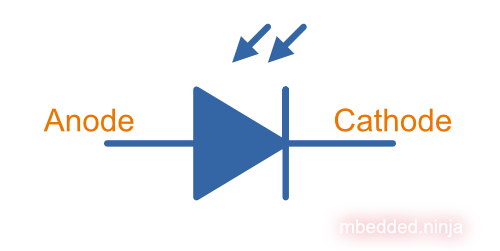
Schematic Symbol
The schematic symbol below is the common one used for a photodiode.
Types of Photodiodes
There are three basic types of photodiode:
- PN junction photodiode
- PIN photodiode
- Avalanche photodiode
PN Junction Photodiode
A PN junction photodiode is the “standard photodiode” that uses a PN junction to detect light. The PN junction forms a depletion region, which is exposed to the environment through a transparent window. When a photon strikes this depletion region, it is absorbed, and an electron-hole pair is created. Because of the electric field present in the depletion region, the electron will want to move (swept) towards the N doped semiconductor, whilst the hole will want to move towards the P doped semiconductor. These moving charge carriers create the photodiode current (photocurrent) that you measure.
PIN Photodiode
A PIN photodiode is a variant of the standard PN junction photodiode that has an intrinsic layer placed between the two doped semiconductor layers. This intrinsic region increases the depletion region, which in turn reduces the junction capacitance of the photodiode. This allows it to be used in high-speed applications.
Avalanche Photodiode
An avalanche photodiode (APD) is a variant of the standard PN junction photodiode that makes use of impact ionization (the avalanche effect) to increase the photon to current response of the photodiode (gain). This internal gain means that APDs have high responsivity, making them useful for detecting extremely low levels of light. APDs must be operated at a high reverse-bias voltage, near their breakdown voltage. Even though the high reverse-bias creates a larger dark current (and higher current noise), the effect of the internal gain outweighs this additional noise, making them suitable for low-level light detection.1
Photodiode Current vs. Voltage
The typical relationship between the photodiode’s voltage and current is shown in the graph below.
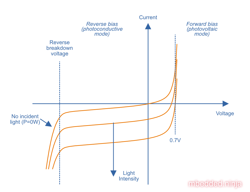
The top-most curve is when there is no incident light (). You will notice this curve goes through . As the incident light power increases, the curve shifts downwards, in a mostly linear fashion (this is why you can make accurate light sensors with photodiodes).
The right-half of the graph is not terribly interesting, as the photodiode just acts as a normal diode in this area, with a sharp increase in the current around the typical “turn-on” voltage of . In the left-hand side of the graph, as the reverse-bias voltage increases, the diode’s dark current increases (the line with ).
Important Parameters
Responsivity
- Units:
- Typical range:
Linearity
In some cases, applying a reverse voltage is effective in enhancing the upper limit of linearity — Hamamatsu: Si photodiodes2.
Quantum Efficiency
Spectral Range
- Units:
- Typical range:
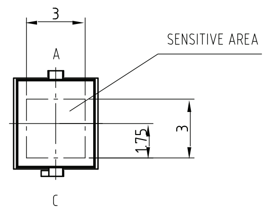
Sensitive Area
- Units:
- Typical range:
The sensitive area is the area of the PN junction that is exposed and responds to light. A larger sensitive area will result in a photodiode being able to detect lower levels of light, and provide more bits of resolution.
Dark Current
The dark current for a silicon photodiode approximately doubles for every in temperature rise, giving rise to the following equation:4
The dark current at is usually specified in the photodiode’s datasheet. Using this equation, you can then find the dark current for any other temperature.
Basic Photodiode-based Transimpedance Amplifier Circuit
Photodiodes are commonly used to measure light intensities. But the output of a photodiode is a very small current (typically ), which isn’t very useful for measuring. A common “analogue front-end” to add to a photodiode is a transimpedance amplifier using an op-amp, as shown in the schematic below. The transimpedance amplifier converts the very small current into a much larger voltage. This voltage can then be used to control other parts of a circuit or can be fed into an ADC for digitizing before being read by a microcontroller.
Because the op-amp’s non-inverting input is tied to ground, the inverting input is a “virtual ground” (it also stays at ). Because the diode current has no-where to go but through the resistor , this gives the simple equation:
It’s important to pay attention to the input bias current when choosing the op-amp for this circuit. This is because the photodiode sources a very small current (e.g. in the ). Any input bias current is either going to add or subtract from this photodiode current before being amplified by the feedback resistor. Jellybean op-amps have in the range of . You normally want to pick an op-amp which has an input bias current that is at least an order of magnitude smaller than the photodiode current you are trying to measure. Luckily, you can get op-amps that are specifically designed to have small input bias currents. For example, the Texas Instruments OPA396 has a typ. at ! This increases to approx. across its entire temperature range (typical).5
An alternative to using a transimpedance amplifier to convert current to voltage is to use an op-amp and a capacitor to act as an integrator. You can buy special switched capacitor ICs that package the op-amp, switches and precision capacitor in a single semiconductor IC. They offer good SNR, but with relatively low bandwidth.6 However, this method is not as popular as the transimpedance amplifier, and the dedicated ICs are expensive and hard to source.
The current noise density of the circuit is:7
where:
is the current noise density, in
is Boltzmann’s constant,
is the temperature of the photodiode, in
Gain Peaking Capacitor
A capacitor can be added in parallel with to prevent gain peaking.
Biasing
When connected to a transimpedance amplifier, the photodiode can either be used with potential across it (photovoltaic mode) or with a reverse bias (photoconductive mode).7
Photovoltaic Mode
Photovoltaic mode is when the photodiode is not operated with any DC bias across it (i.e. there is across it). This is usually achieved by tying one side of the photodiode to ground, whilst the other side is held at “virtual ground” by an op-amp.
The photovoltaic mode of operation is recommended for low speed () and low-light level applications.7 It also appears to be more linear, due to the smaller variations in response from changes in temperature.7
Photoconductive Mode
Photoconductive mode is when the photodiode is operated with a reverse-bias voltage across it. Applying a reverse-bias to a photodiode can improve the speed of the device, and is the preferred mode of operation for high-speed applications.7 The speed increase is because a greater reverse-bias increases the depletion region. This in turn reduces the junction capacitance, increasing the bandwidth of the device.
- Increased speed.
- Increased dark and noise current.
Equivalent Circuit
The equivalent circuit below can be used to model a photodiode.
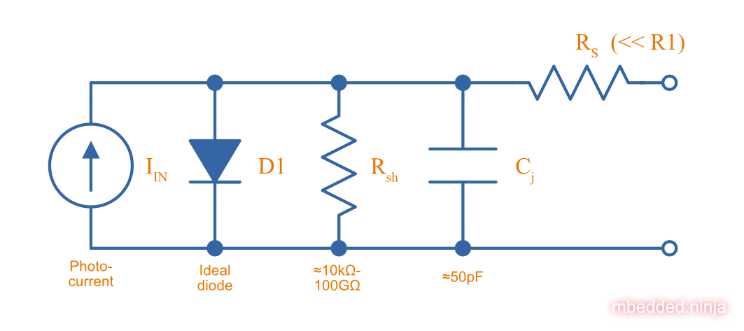
represents the resistance in parallel with the current source, and is called the shunt resistance. You want this shunt resistance to be as high as possible, as this means more of the current is delivered to the load. Germanium photodiodes can have lower shunt resistance in the range.8
represents the series resistance of the photodiode, arising from the resistance of the semiconductor material and the contacts. You want this to be as low as possible (it is much smaller than the shunt resistance ).
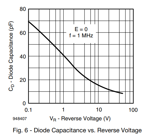
represents the junction capacitance, caused by the depletion region of the PN junction. Junction capacitance affects the photodiode’s high-frequency response, as the capacitance’s impedance drops with increasing frequency. Lower capacitance photodiodes have better high frequency response. The value of is not constant — in fact it is strongly dependent on the reverse-bias voltage. The higher the reverse-bias, the lower the capacitance. Thus you can improve a photodiodes high frequency response by reverse-biasing it at a high voltage.
Manufacturers
Opto Diode
Opto Diode manufacture a range of silicon photodiodes in through-hole TO-5, TO-8 and TO-18 packages.
Popular Parts
Vishay BPW34
- Package: DIP-2
- Price: US$0.48 (1000)
Popular PIN photodiode with a spectral range from .
Footnotes
-
Wavelength Electronics (2018). Photodiode Basics [article]. Retrieved 2022-02-28, from https://www.teamwavelength.com/photodiode-basics/. ↩
-
Hamamatsu (2020, Dec). Si photodiodes [datasheet]. Retrieved 2022-02-28, from https://www.hamamatsu.com/content/dam/hamamatsu-photonics/sites/documents/99_SALES_LIBRARY/ssd/si_pd_kspd9001e.pdf. ↩
-
Vishay (2011, Aug 23). BPW34, BPW34S: Silicon PIN Photodiode [datasheet]. Retrieved 2022-02-27, from https://www.vishay.com/docs/81521/bpw34.pdf. ↩ ↩2
-
Wei-Chih Wang. Optical Detectors [lecture notes]. Retrieved 2022-03-02, from https://depts.washington.edu/mictech/optics/me557/detector.pdf. ↩
-
Texas Instruments (formerly Burr-Brown) (2021, Jul). OPA396 Precision, Low IQ, Low Input Bias Current Op Amp [datasheet]. Retrieved 2022-10-10, from https://www.ti.com/lit/ds/symlink/opa396.pdf. ↩
-
Bonnie C. Baker (1993). Comparison Of Noise Performance Between A FET Transimpedance Amplifier And A Switched Integrator [application note]. Burr-Brown (now Texas Instruments). Retrieved 2022-02-25, from https://www.ti.com/lit/an/sboa034/sboa034.pdf. ↩
-
OSI Optoelectronics. Photodiode Characteristics and Applications [application note]. Retrieved 2022-02-27, from http://www.osioptoelectronics.com/application-notes/an-photodiode-parameters-characteristics.pdf. ↩ ↩2 ↩3 ↩4 ↩5 ↩6
-
Robert Keim (2020, Dec 23). Understanding the Photodiode Equivalent Circuit [article]. All About Circuits. Retrieved 2022-02-27, from https://www.allaboutcircuits.com/technical-articles/understanding-the-photodiode-equivalent-circuit/. ↩
-
Opto Diode (2022, Jan 27). Photodiode 5 mm2 - Isolated: ODD-5WISOL [datasheet]. Retrieved 2022-02-27, from https://optodiode.com/pdf/ODD-5WISOL.pdf. ↩