Buck Converters

Buck converters are a particular topology of switch-mode power supply (SMPSs) that use a switching element, diode (or second switch), inductor and capacitor to convert an input voltage into a lower output voltage.

To learn more about EMI/EMC considerations regarding buck converters, see the EMC Design Guidelines page.
How A Buck Converter Works
The output voltage of a buck converter is purely determined by the input voltage and the percentage of time that the switch spends in the on-state during each switching cycle, :
is the duty cycle, and varies from to . It is defined as:
where:
is the on time of the switch, in seconds
is the switching period, in seconds ()
The following steps show a way to intuitively understand how a buck converter produces a lower output voltage (and derive the basic equation):
- The average voltage across the inductor, over an entire switching cycle, must be 0 (other ways of saying is this is that the integral must be 0, or the volt-seconds must be 0). If it wasn’t, then because (the basic equation for an inductor), the current in the inductor would increase or decrease without bound (i.e. go to infinity).
- When the switch is closed (), the voltage across is during this phase.
- When the switch is open (), is forward biased, and if we assume it’s a perfect diode (no forward voltage drop), the voltage across is during this phase.
- The average (or integral) over the entire switching cycle has to be 0, so:
When the switch is closed, the current flows from the input through the inductor to the output, as shown below:

When the switch opens, the input is disconnected. Because the inductor doesn’t like changes in current, it keeps a current flowing through the load by forward biasing , as shown below:

(which is also called ) is to reduce the voltage ripple at the output/load.
Control Methods
99% of the time, you want a fixed (regulated) and stable output voltage, which does not depend on the input voltage and one which does not start to sag as you draw more current. To achieve this, it is insufficient to drive the switch at a fixed duty cycle. More complex control mechanisms with feedback are required. The most popular two are voltage-mode control and current-mode control, which are explained in the following section.
Voltage Mode Control
Voltage-mode (VM) control is the simplest control method, originating in approx. the 1970’s1. It works by taking a proportion of the output voltage and comparing it with a fixed reference voltage. The difference between these two is called the error voltage and is amplified by an error amplifier. This error voltage is then fed into a comparator, with the other input being a sawtooth signal (triangular waveform). The switch is turned on at the start of the sawtooth period, and turned off when the sawtooth exceeds the error voltage. An SR latch is normally used to prevent multiple triggers per cycle due to noise. Voltage-mode control is named as such because the duty cycle is proportional to the control voltage.

Current-Mode Control (Constant Frequency)
Current-mode (CM) control is a very common control method for buck converters.
It has the following advantages over VM:
- Simpler external frequency compensation than VM
- Faster load transient response than VM.
However, one big disadvantage is the extra control circuitry complexity. However, this is somewhat mitigated in more recent years as all of this circuitry is integrated into a cheap silicon IC.
Peak current measurement is a common way of “measuring” the average output current.
A transconductance amplifier (amplifier that converts a input voltage to an output current) is used to compare the voltage at a feedback pin (typically labelled FB) to an internal voltage reference.
PCM: Peak current mode
See the excellent SNVA555: Understanding and Applying Current-Mode Control Theory by TI for more information on current-mode control theory.
Hysteretic Control
Hysteretic control is when the output voltage is directly monitored by a comparator, rather than going through an error amplifier. If the output voltage falls or exceeds below a certain value, the buck converter switch is turned on/off. Because the control is performed by measuring the ripple in the output voltage, this method is also called the ripple control method.
There are two ways on controlling the switch:
- Detect when the voltage falls BELOW a set threshold, and turn the switch ON for a fixed amount of time, OR
- Detect when the voltage rises ABOVE a set threshold, and turn the switch OFF for a fixed amount of time
Hysteretic control has the benefit of being extremely fast to respond to transient current changes, since it is directly monitoring the output voltage and there is no error amplifier. It also does not need any compensation. These advantages make it suitable for powering the rapidly changing current demands of high power CPUs and FPGAs.
Calculating Buck Converter Component Values
Inductor Selection
You can use the following equations to select the inductor for a buck converter.
In a buck converter the inductor is in series with the output, so the average inductor current is equal to the average output current:
where:
is the output current of the buck regulator (pick your maximum)
Then, calculate the value of inductance required with:2
where:
is the input voltage to the buck regulator
is the output voltage of the buck regulator
= the desired ripple current in the inductor
= the switching frequency
The ripple current is typically chosen to be 20-40% of the average current2. If we choose 30%, then we can calculate with:
Capacitor Selection
The output capacitance is primarily determined by the maximum allowed output voltage ripple. This ripple is determined by the capacitance of the capacitor and its ESR (equivalent series resistance). The minimum output capacitance for a buck converter can be found using:2
where:
= the inductor ripple current (from above)
= the maximum desired output voltage ripple
= the switching frequency
The actual ripple will be slightly larger than this due to the ESR of the capacitor. The output capacitor carries the inductor ripple current, so the ESR contributes an additional ripple voltage of:
where:
= the parasitic series resistance of the output capacitor
The total output ripple is the sum of the ripple caused by the capacitance, and the ripple caused by the ESR.
Buck Converter Calculator
Use the generic buck-converter design helper below to compute the duty cycle and required inductance from the supply/output voltages, diode and switch drops, switching frequency, output current and acceptable inductor ripple.
MP4558 Design Tool
The MP4558 is a buck converter IC from Monolithic Power Systems. The calculator below applies the design equations directly from its datasheet to size the frequency-setting resistor, feedback divider, inductor and capacitors for your target output voltage, switching frequency and load. The internal feedback reference voltage is .
Pick your switching frequency, set the bottom feedback resistor () to a value you’d actually like to use (typically ), and the tool computes everything else.
Synchronous Rectification
When using a P-channel MOSFET for synchronous rectification, its body diode is forward-biased when the converter is in shutdown mode. This can drain the power source into the output. More advanced buck converters have extra circuitry to disconnect this P-channel MOSFET when the device is not active.
EMC
The input current “hot loop” of a buck converter is the most important part to worry about when it comes to EMC. See the EMC Design Guidelines page for more information.
Examples
Tiny (Nano) Buck Converters
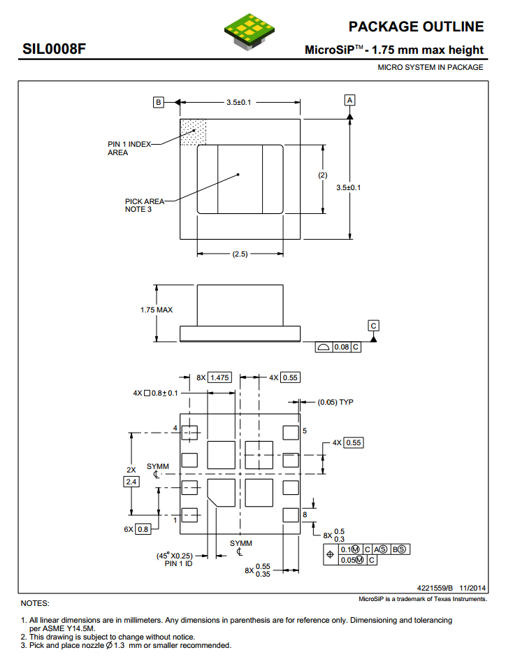
Texas Instruments released a series of very small (3.5x3.5x1.8mm) buck converter modules in 2015. One of the most impressive features is that this includes the inductor (external capacitors are still required). One example is the LMZ20502, which can provide up to 2A of current with an input voltage range of 2.7-5.5V and a output voltage range of 0.8-3.6V.
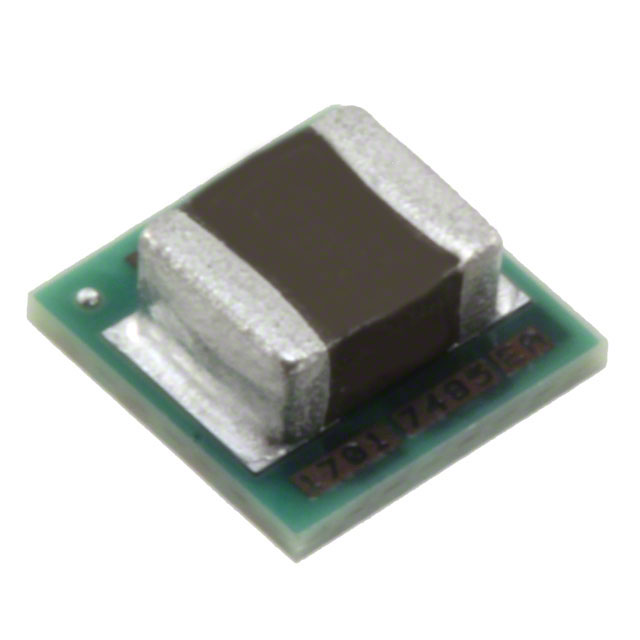
Notice how most of the volume on the module is taken up the chip inductor (the big brown thing that dominates most of the image). The dimensions of the package are shown in the diagram below.
Footnotes
-
Maniktala, Sanjaya (2012). Voltage-Mode, Current-Mode (and Hysteretic Control). Microsemi. Retrieved 2021-08-22, from https://www.microsemi.com/document-portal/doc_view/124786-voltage-mode-current-mode-and-hysteretic-control. ↩
-
Brigitte Hauke (2015, Aug). Basic Calculation of a Buck Converter’s Power Stage [Application Report]. Texas Instruments. Retrieved 2023-06-20, from https://www.ti.com/lit/an/slva477b/slva477b.pdf. ↩ ↩2 ↩3