Most electronic components come in standardized packages. A package type has well a defined set of physical dimensions that the component has to conform to. For each package, normally the pitch spacing, height and general shape is defined. However most packages contain variants with a differing number of leads (for example the classic old-school DIP package comes in 4, 8, and 10 lead variants just to name a few). This means that total land area and size of a package can vary according to how many leads it has.
Standardizing components sizes and shapes makes it easier for the component manufacturer, the PCB manufacturer, and the design engineer. Although most components are standardized, there are still plenty of packages out there. This pages purpose is to hopefully make some sense of the most common and widely used packages and to help anyone choosing a component package or designing a PCB.
Component Package Database
Packages are listed alphabetically below. Click on any package to see more information.
All land-area (occupied PCB space) calculations are based around the minimum-sized square that encloses the entire package. This does not take into account the size of the pads required on the PCB, which would increase the calculation by a small amount. Nominal package dimensions used for calculation.
Click on any photo to expand into a full-sized version.
Component packages with many names (synonyms) are listed by the most common, or most “popular” name, which is not necessarily the technically correct name.
Some items such as the PP3 9V battery case , and SIM card sizes , may not be strictly component packages, but are included here for completeness.
2-3AB1A Component Package
2-3AB1A Component Package
463C-03 Component Package
463C-03 Component Package
BCC is a variant within the chip carrier package family.
BCC Component Package BCC is a variant within the chip carrier package family.
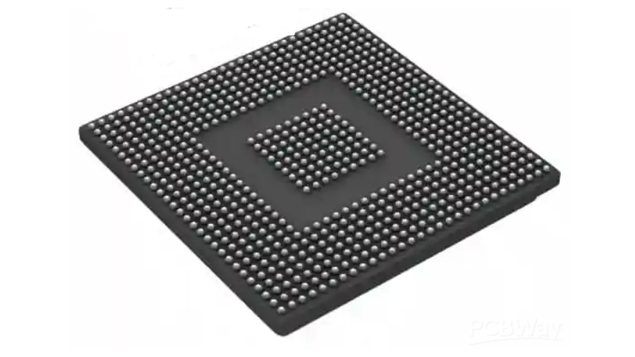
BGA is a high-density SMD component package which can have from 4 to 1700+ pins. The pins are solder balls which are arranged in a grid on the underside of the package.
BGA Component Package BGA is a high-density SMD component package which can have from 4 to 1700+ pins. The pins are solder balls which are arranged in a grid on the underside of the package.
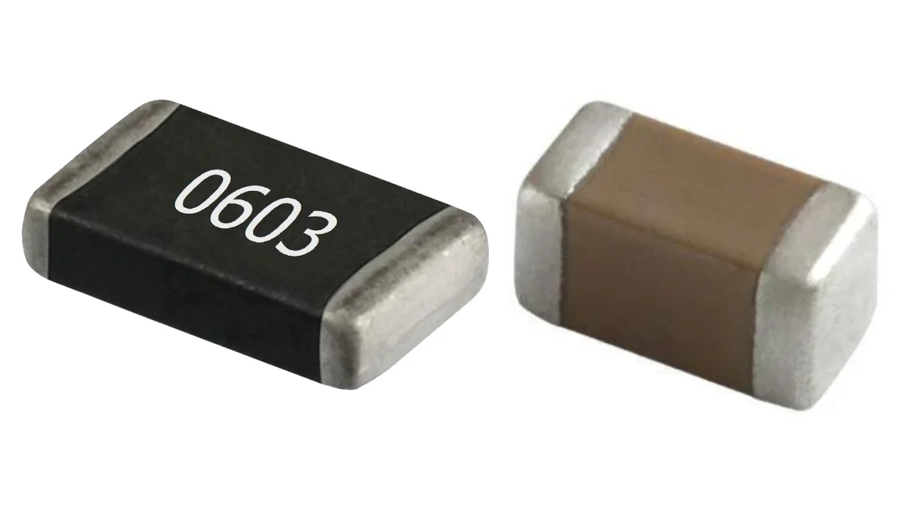
Chip (EIA) Component Packages Chip (EIA xxxx) components are family of very popular rectangular SMD cuboid packages, commonly used for resistors and capacitors.
Chip (EIA) Component Packages Chip (EIA xxxx) components are family of very popular rectangular SMD cuboid packages, commonly used for resistors and capacitors.
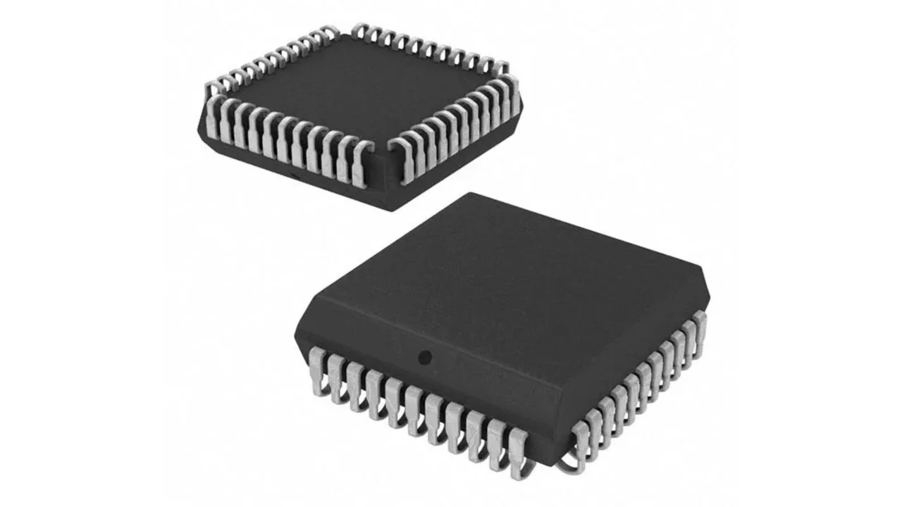
Chip carrier packages are a family of large SMD packages that hold ICs with leads on all four sides of the package. One of the most common variants is the PLCC package with J leads.
Chip Carrier Packages Chip carrier packages are a family of large SMD packages that hold ICs with leads on all four sides of the package. One of the most common variants is the PLCC package with J leads.
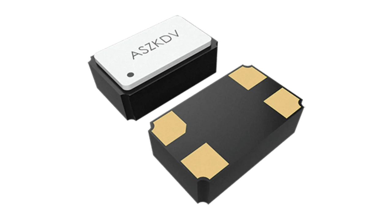
Crystals come in a variety of through-hole and SMD packages. Older crystals use through-hole packages that looked like shiny metal cans, where modern crystals usually come in small SMD packages with 2 or 4 leads and look like ICs.
Crystal Packages Crystals come in a variety of through-hole and SMD packages. Older crystals use through-hole packages that looked like shiny metal cans, where modern crystals usually come in small SMD packages with 2 or 4 leads and look like ICs.
D2PAK is a synonym for the TO-263 component package.
D2PAK Component Package D2PAK is a synonym for the TO-263 component package.
D3PAK is a synonym for the TO-268 component package.
D3PAK Component Package D3PAK is a synonym for the TO-268 component package.
DDDPAK is a synonym for the TO-268 component package.
DDDPAK Component Package DDDPAK is a synonym for the TO-268 component package.
DDPAK is a synonym for the TO-263 component package.
DDPAK Component Package DDPAK is a synonym for the TO-263 component package.
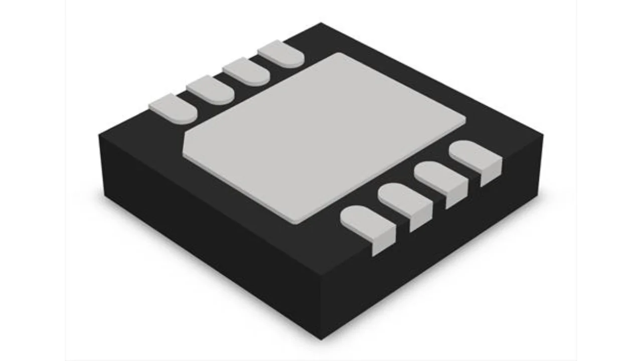
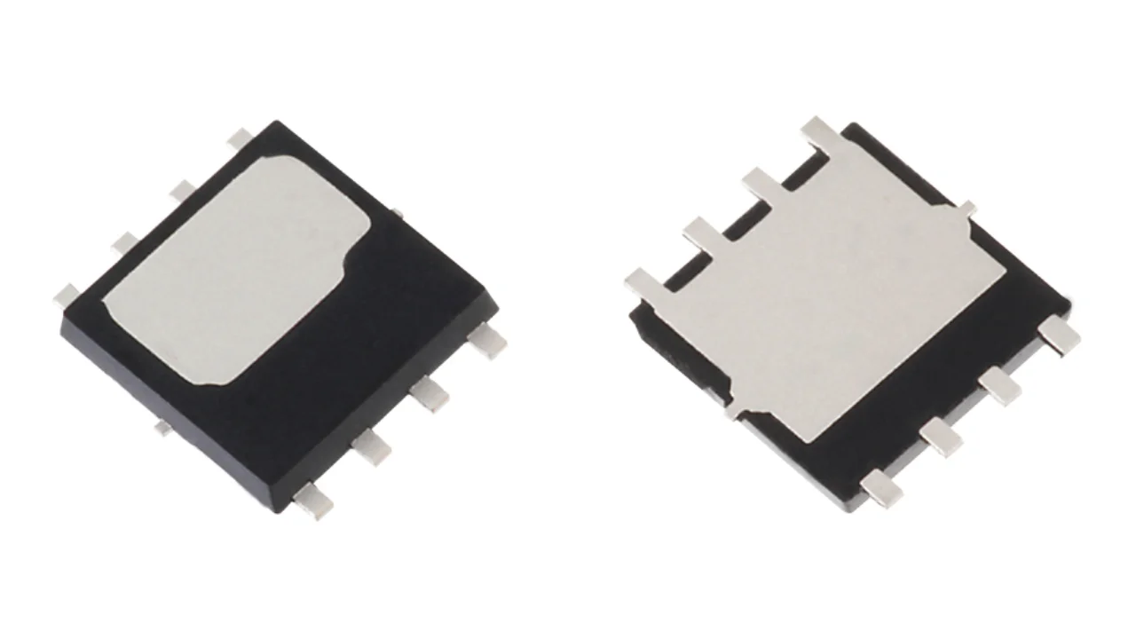
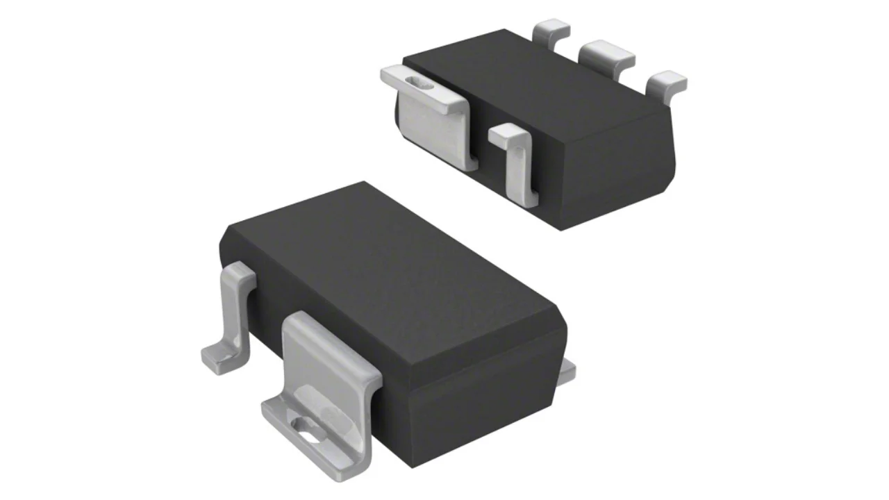
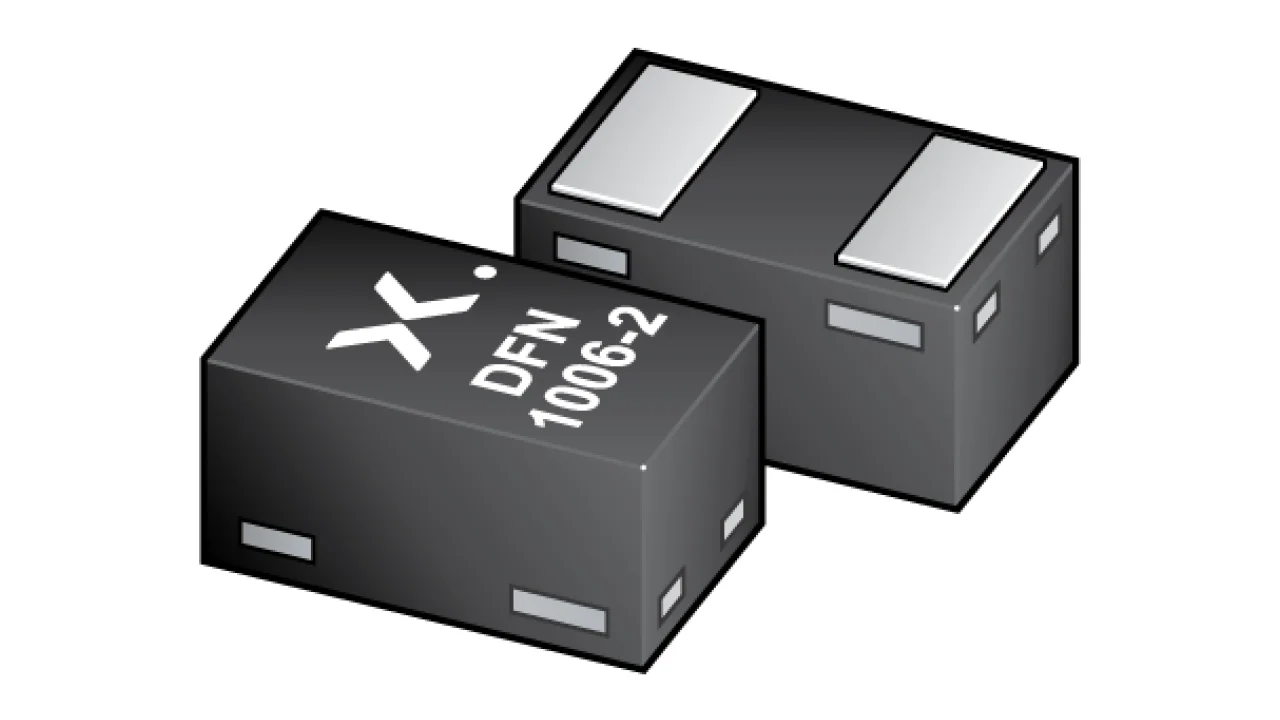
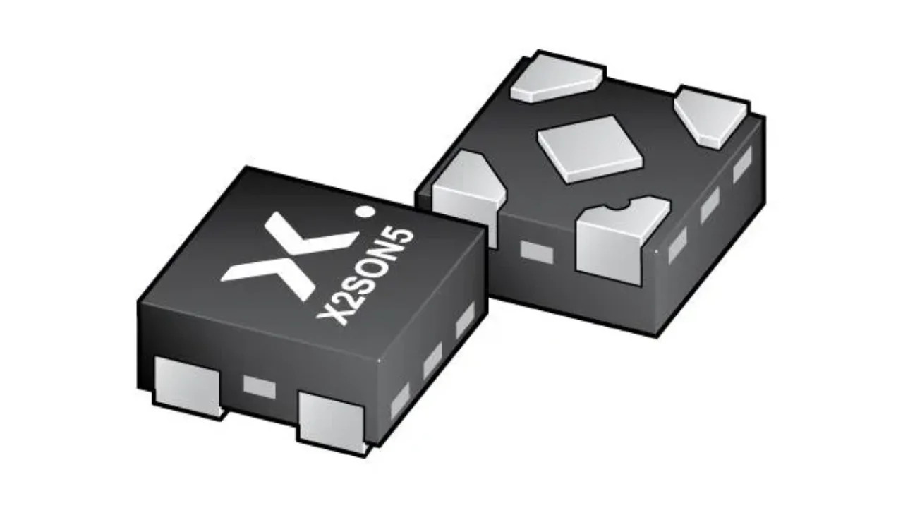
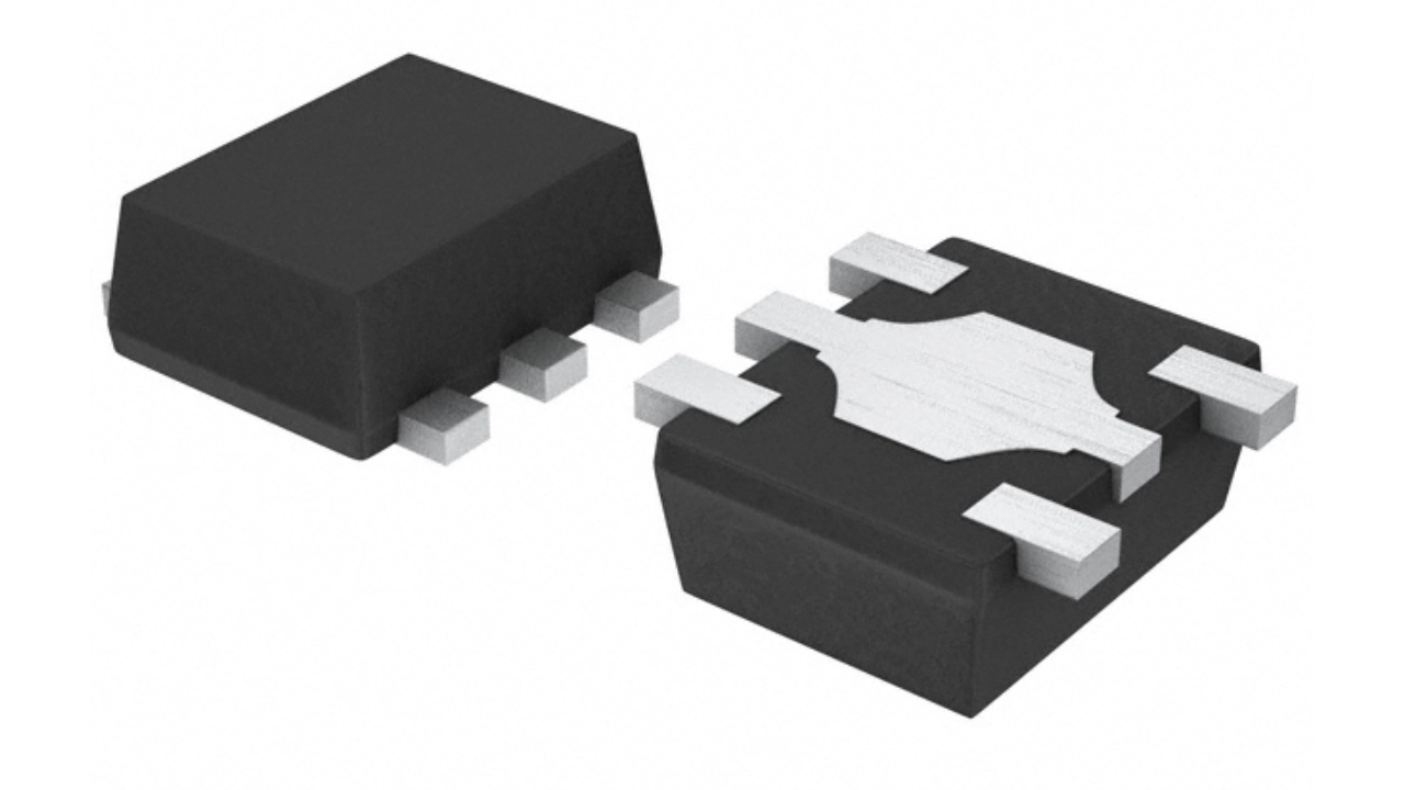
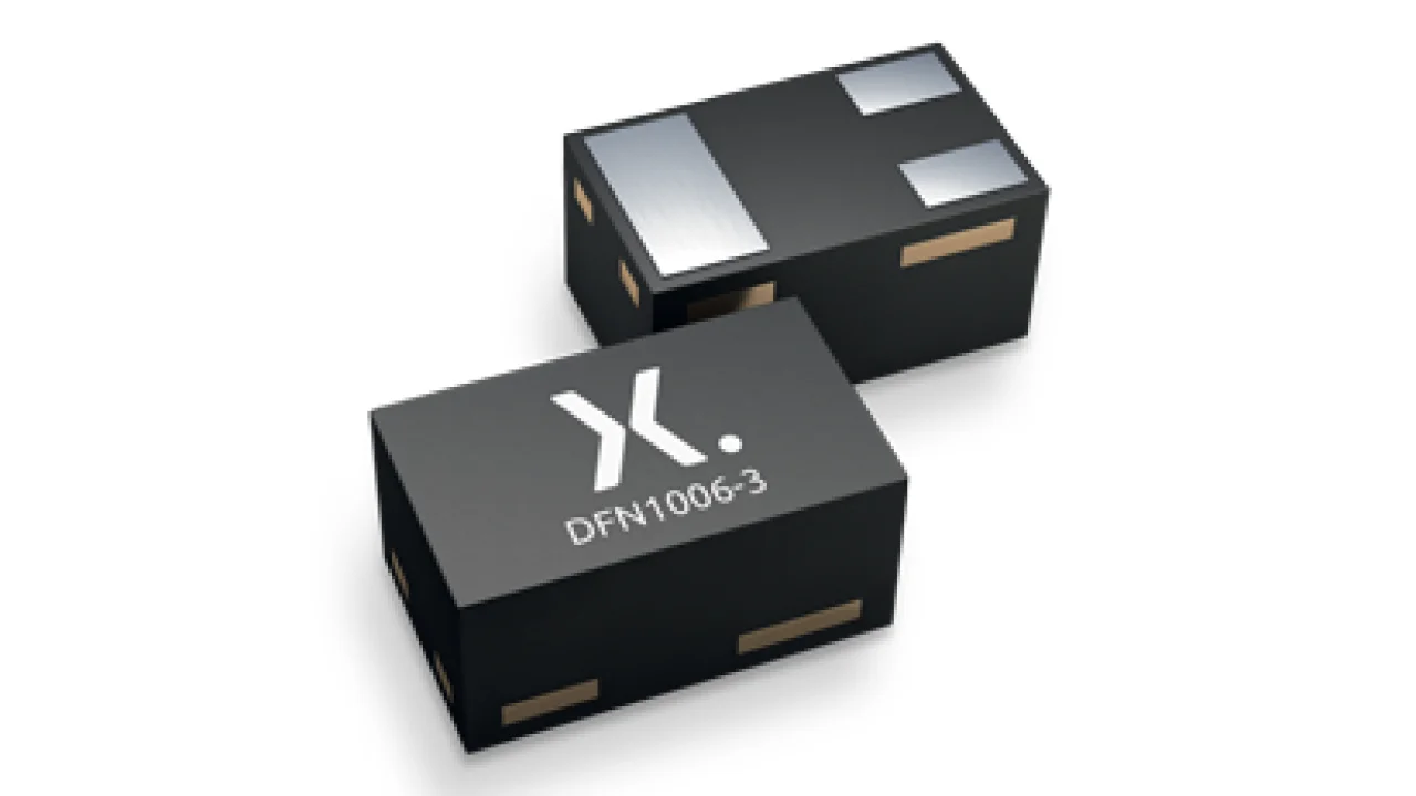
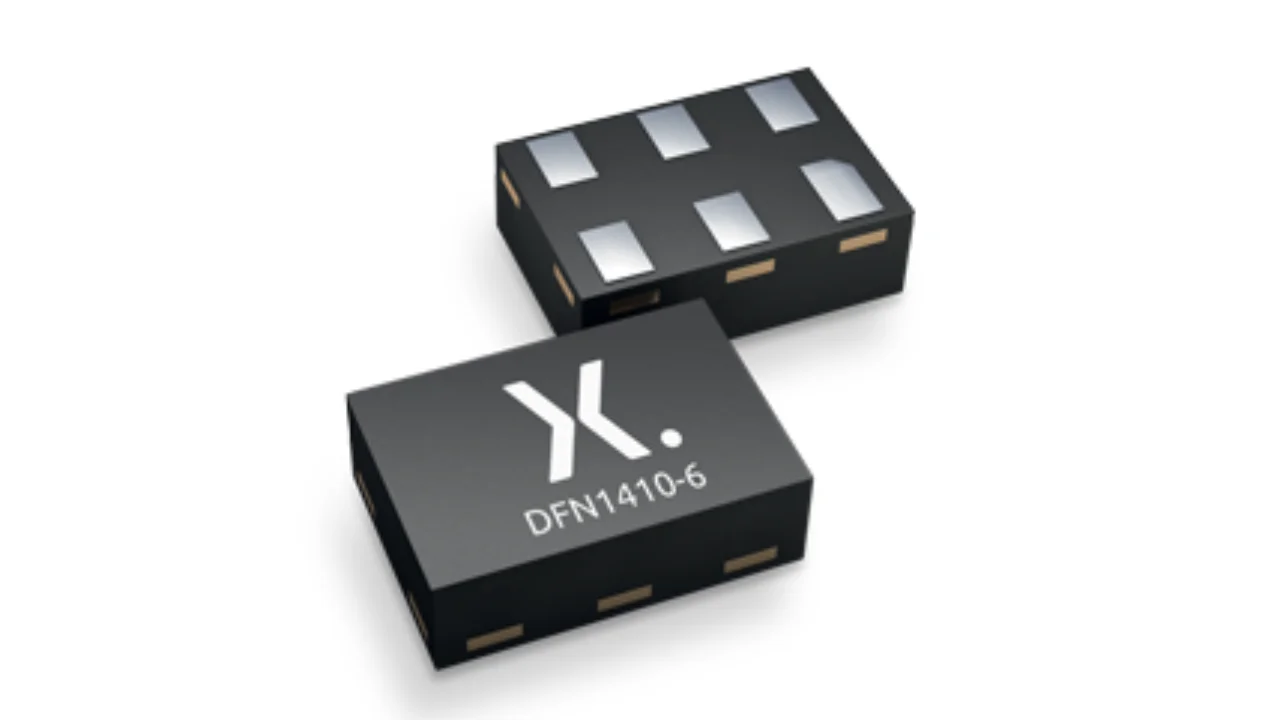
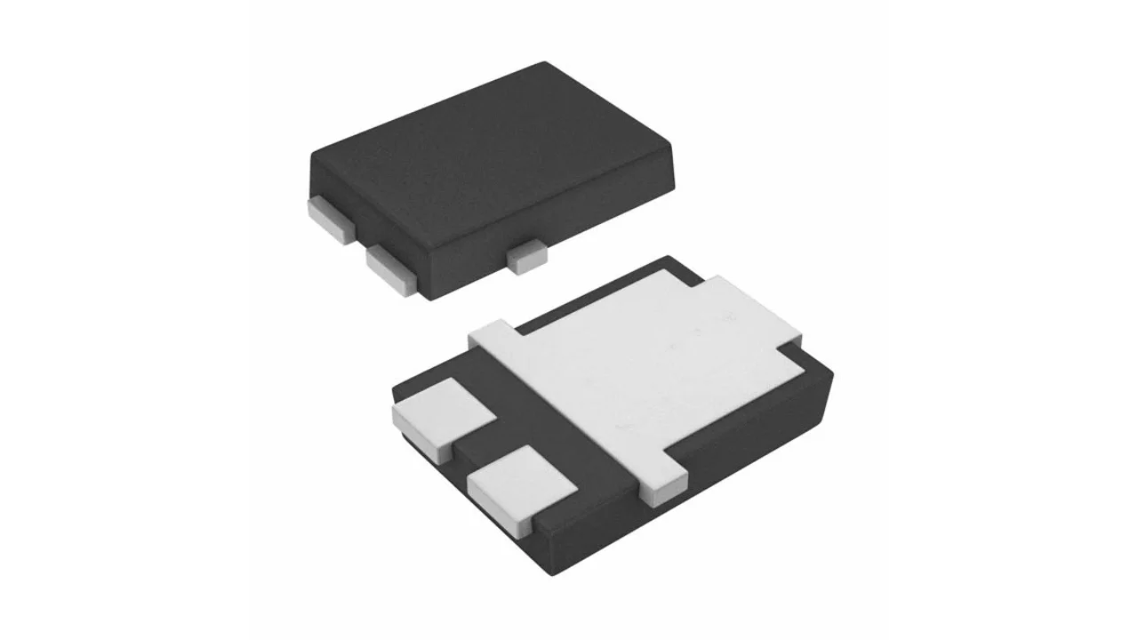
DFN (a.k.a. SON) is a popular SMD component package with pins running down two of its sides. It is commonly used for MOSFETs, flash memory ICs and other devices.
DFN Component Package DFN (a.k.a. SON) is a popular SMD component package with pins running down two of its sides. It is commonly used for MOSFETs, flash memory ICs and other devices.
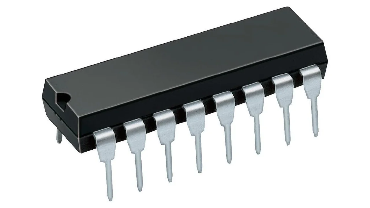
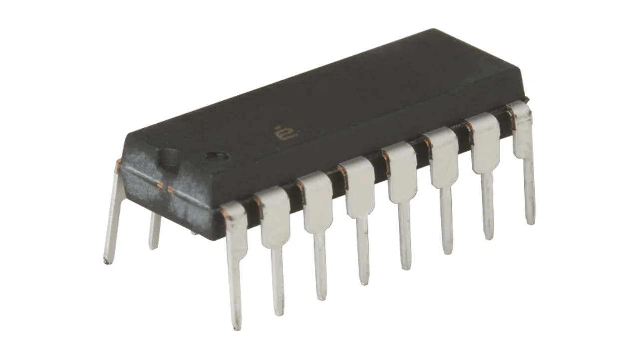
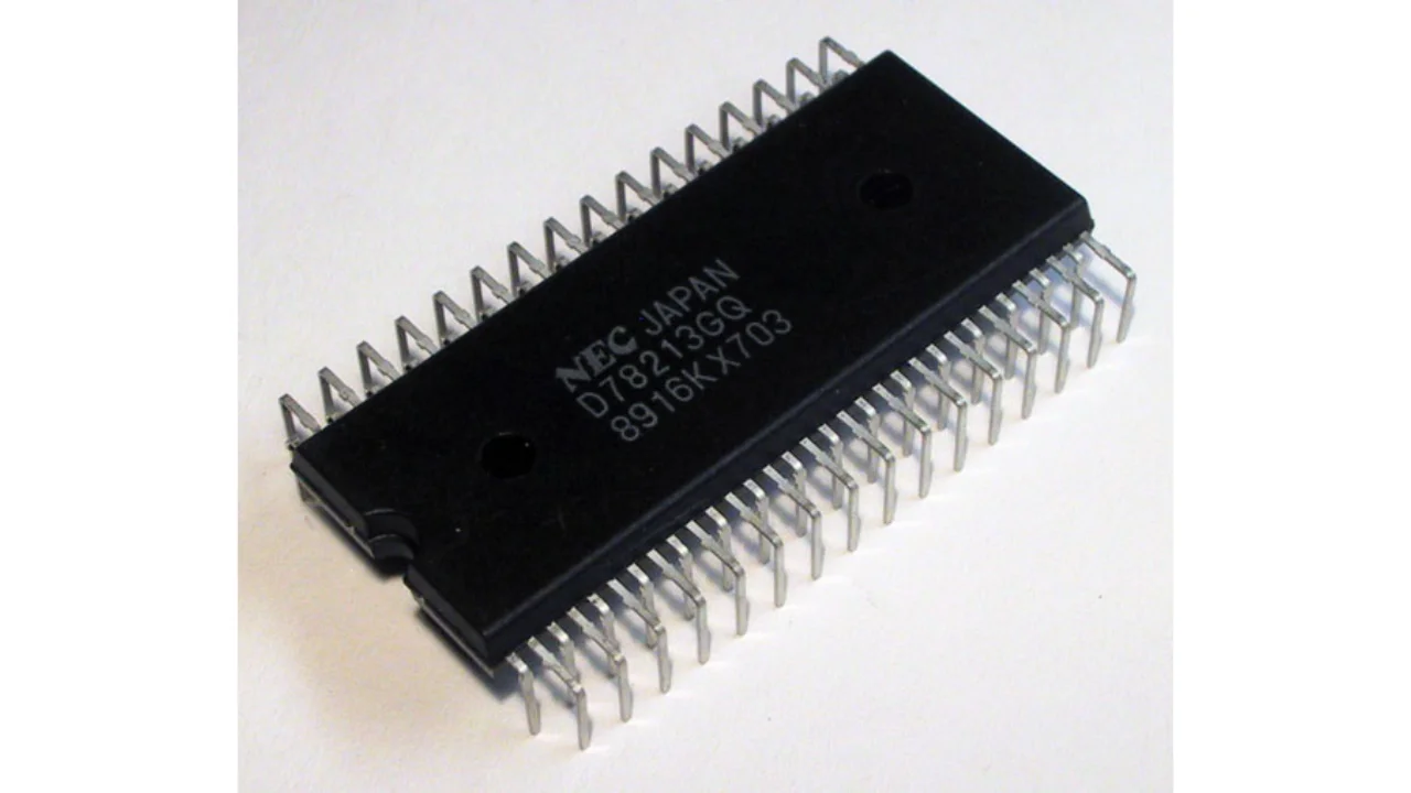
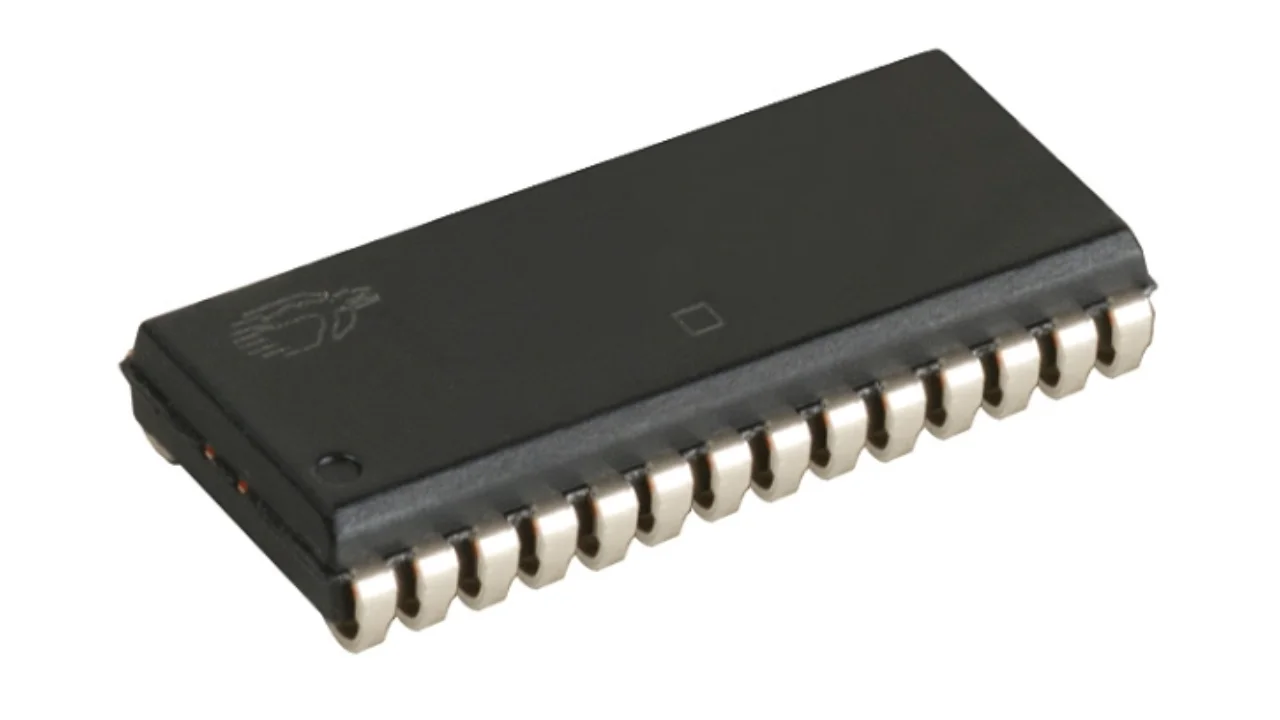
DIP is an popular through-hole component package typically used for ICs.
DIP Component Package DIP is an popular through-hole component package typically used for ICs.
DO-103AA Component Package DO-103AA is a synonym for the MiniMELF component package.
DO-103AA Component Package DO-103AA is a synonym for the MiniMELF component package.
DO-103AB Component Package DO-103AB is a synonym for the MELF component package.
DO-103AB Component Package DO-103AB is a synonym for the MELF component package.
DO-14 is a synonym for the DO-204AB component package.
DO-14 Component Package DO-14 is a synonym for the DO-204AB component package.
DO-15 is a synonym for the DO-204AC component package.
DO-15 Component Package DO-15 is a synonym for the DO-204AC component package.
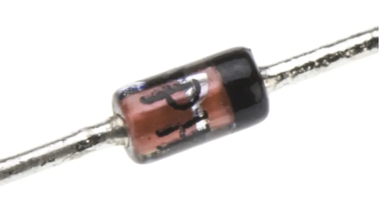
DO-204AA (DO-7) Component Package DO-204 (a.k.a. DO-7) is an older 2-lead hermetically sealed glass through-hole package used for diodes.
DO-204AA (DO-7) Component Package DO-204 (a.k.a. DO-7) is an older 2-lead hermetically sealed glass through-hole package used for diodes.
DO-204AB (DO-14) Component Package Dimensions, recommended PCB footprints, variants, synonyms and more for the DO-204AB (DO-14) component package.
DO-204AB (DO-14) Component Package Dimensions, recommended PCB footprints, variants, synonyms and more for the DO-204AB (DO-14) component package.
DO-204AC (DO-15) Component Package DO-204AC (DO-15) is an older through-hole axial component package used for diodes.
DO-204AC (DO-15) Component Package DO-204AC (DO-15) is an older through-hole axial component package used for diodes.
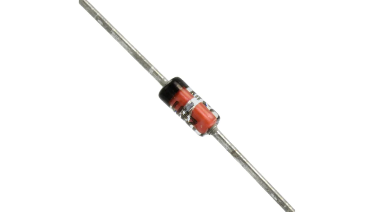
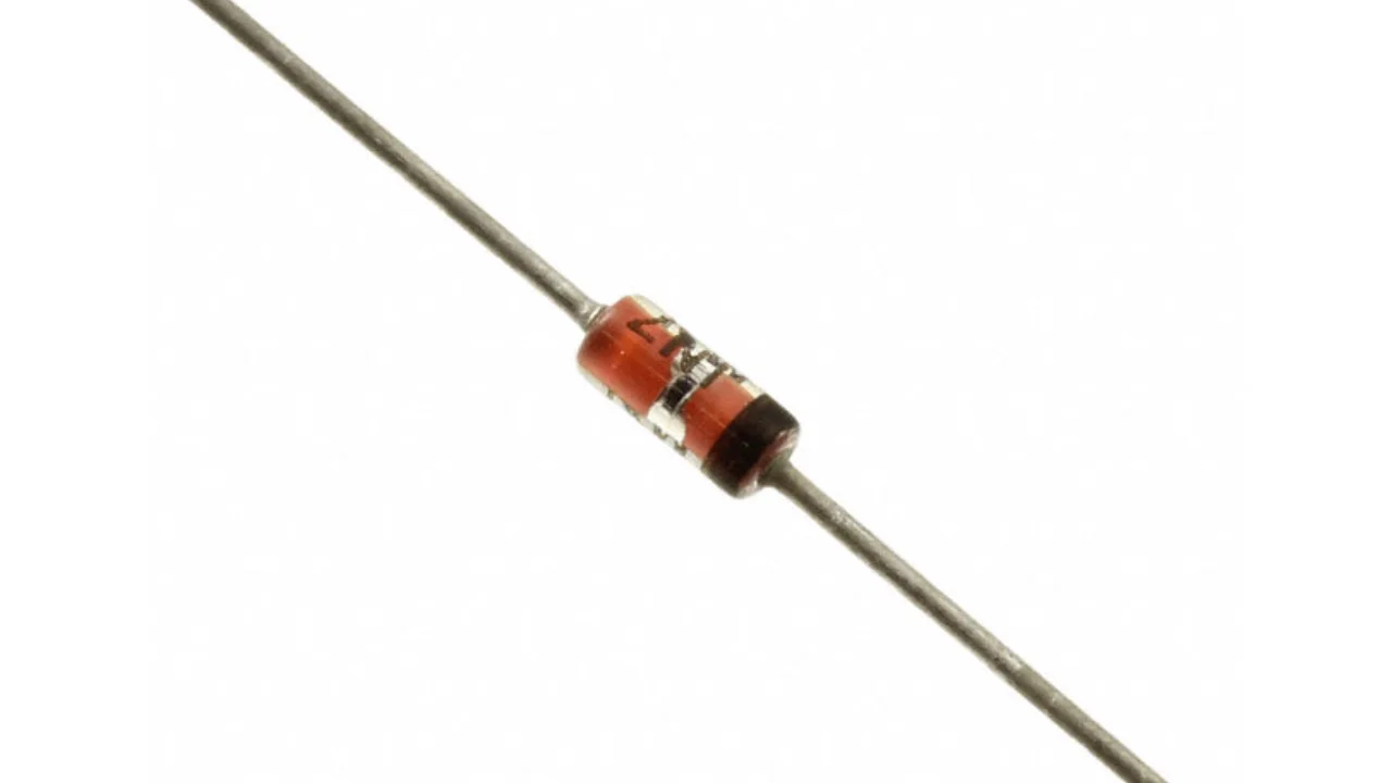
DO-204AH (DO-35) Component Package DO-204AH (DO-35) is an older through-hole axial component package used for diodes. It was commonly used for small-signal low-power diodes such as the general purpose 1N414x series and the Zener BZX55 series.
DO-204AH (DO-35) Component Package DO-204AH (DO-35) is an older through-hole axial component package used for diodes. It was commonly used for small-signal low-power diodes such as the general purpose 1N414x series and the Zener BZX55 series.
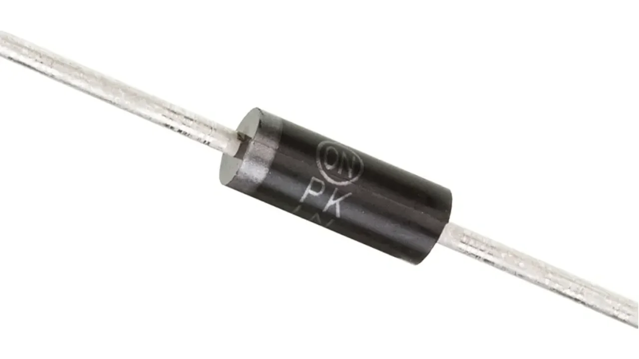
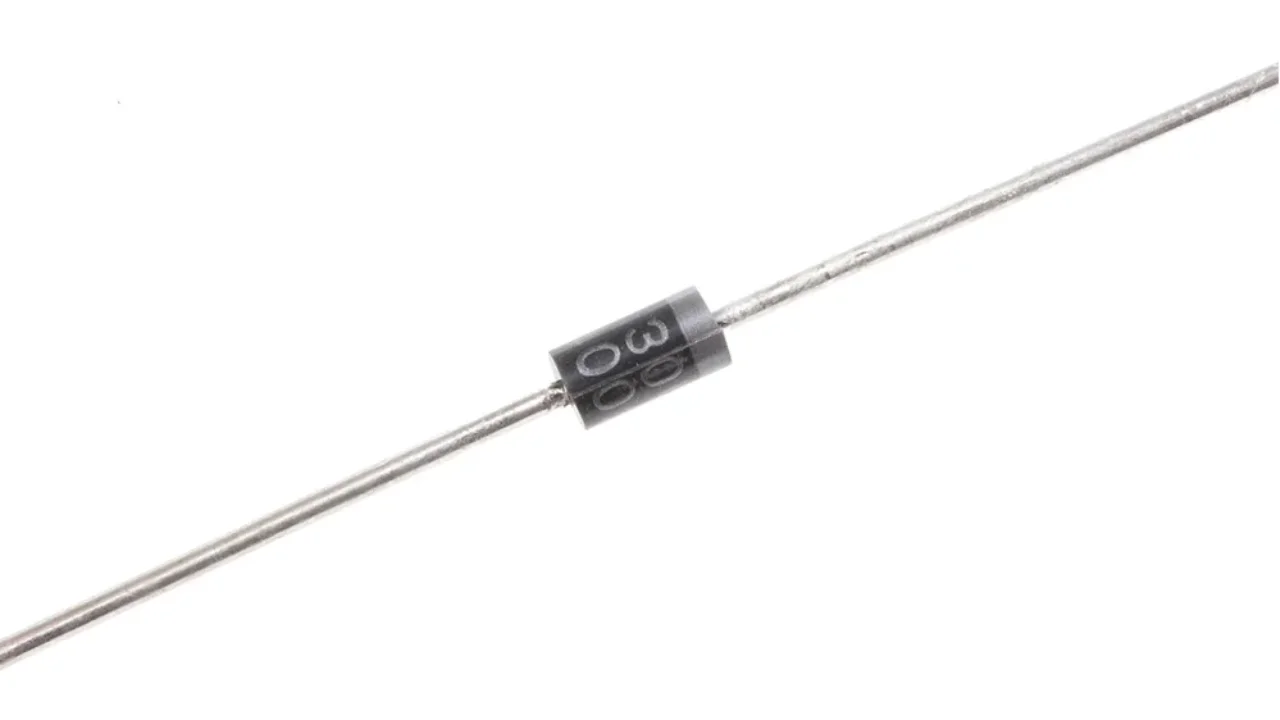
DO-204AL (DO-41) Component Package DO-204AL (DO-41) is a component package commonly used for older through-hole medium current diodes such as the 1N400x series.
DO-204AL (DO-41) Component Package DO-204AL (DO-41) is a component package commonly used for older through-hole medium current diodes such as the 1N400x series.
DO-213AA Component Package DO-213AA (MiniMELF) is a synonym for MiniMELF package.
DO-213AA Component Package DO-213AA (MiniMELF) is a synonym for MiniMELF package.
DO-214AA Component Package DO-214AA (SMB) is a synonym for SMB package.
DO-214AA Component Package DO-214AA (SMB) is a synonym for SMB package.
DO-214AB Component Package DO-214AB is a synonym for the SMC package.
DO-214AB Component Package DO-214AB is a synonym for the SMC package.
DO-214AC Component Package DO-214AC is a synonym for the SMA package.
DO-214AC Component Package DO-214AC is a synonym for the SMA package.
DO-219AA Component Package DO-219AA is a synonym for the SOD-123F package, the flat-lead variant of the SOD-123 package family.
DO-219AA Component Package DO-219AA is a synonym for the SOD-123F package, the flat-lead variant of the SOD-123 package family.
DO-219AB Component Package DO-219AB is a synonym for the SMF package.
DO-219AB Component Package DO-219AB is a synonym for the SMF package.
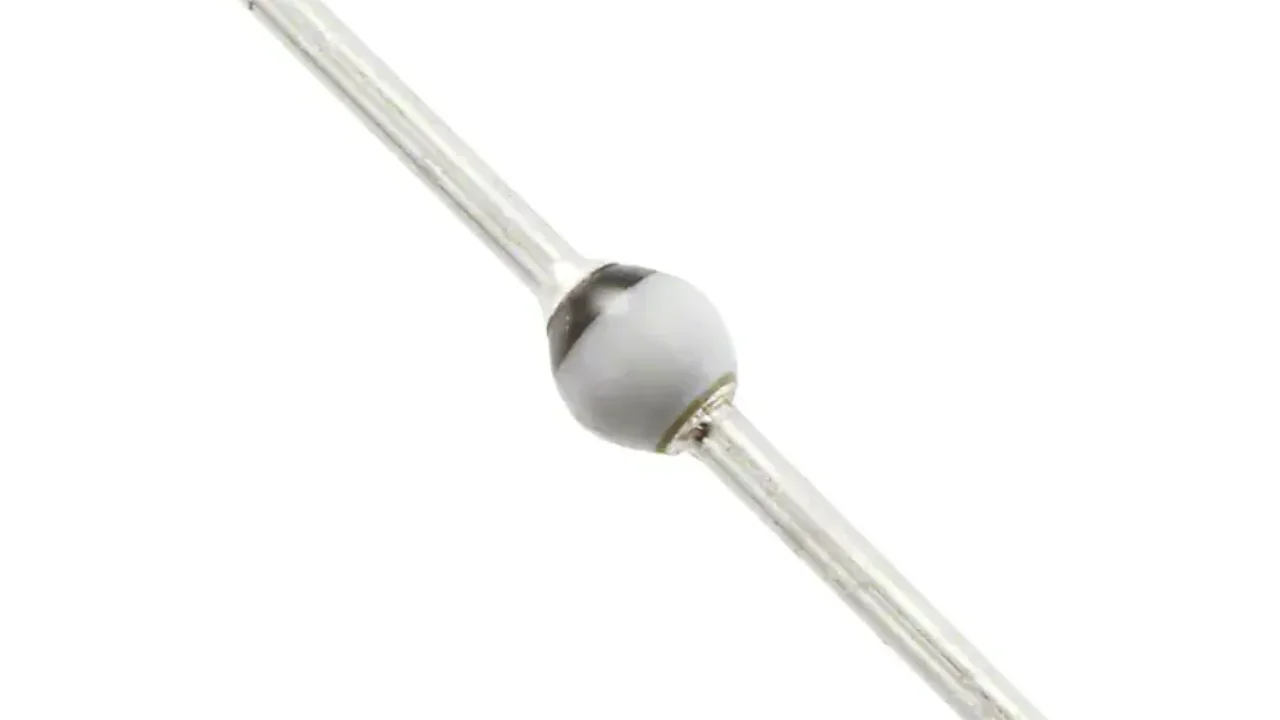
DO-34 (Diode Outline 34) is a hermetically sealed axial 2-lead through-hole glass package used for diodes.
DO-34 Component Package DO-34 (Diode Outline 34) is a hermetically sealed axial 2-lead through-hole glass package used for diodes.
DO-35 (DO-204AH) Component Package DO-35 is a synonym for the DO-204AH package.
DO-35 (DO-204AH) Component Package DO-35 is a synonym for the DO-204AH package.
DO-41 is a older JEDEC name for the DO-204AL component package.
DO-41 Component Package DO-41 is a older JEDEC name for the DO-204AL component package.
DO-7 is a synonym for the DO-204AA component package.
DO-7 Component Package DO-7 is a synonym for the DO-204AA component package.
DPACK is a synonym for the TO-252-3 package.
DPACK Component Package DPACK is a synonym for the TO-252-3 package.
DRL|6 is a synonym for the SOT-563 package.
DRL|6 Component Package DRL|6 is a synonym for the SOT-563 package.
DSOP Advance Component Package DSOP Advance is a SMD component package used by Toshiba that has thermal pads on both the underside and topside of the package.
DSOP Advance Component Package DSOP Advance is a SMD component package used by Toshiba that has thermal pads on both the underside and topside of the package.
E-Line is a through-hole component package that is very similar to the TO-92 package, except it has more of a flat face on one side.
E-Line Component Package E-Line is a through-hole component package that is very similar to the TO-92 package, except it has more of a flat face on one side.
HC-49/US Component Package
HC-49/US Component Package
Pin count, solderability, thermal resistance, dimensions, land pattern, 3D models and more info for the HU3PAK component package.
HU3PAK Component Package Pin count, solderability, thermal resistance, dimensions, land pattern, 3D models and more info for the HU3PAK component package.
Macro X Component Package
Macro X Component Package
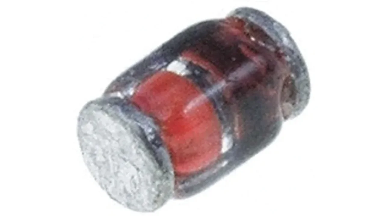
MELF is a 2-lead cylindrically-shaped SMD component package. It is a hermetically sealed glass-based package, which offers components with superb reliability characteristics. They are a pain to solder because they roll around!
MELF Component Package MELF is a 2-lead cylindrically-shaped SMD component package. It is a hermetically sealed glass-based package, which offers components with superb reliability characteristics. They are a pain to solder because they roll around!
Micro SOP Component Package
Micro SOP Component Package
MicroMELF Component Package MicroMELF is a small 2-lead SMD component package. It is the smallest package in the family also containing the MELF and MiniMELF packages.
MicroMELF Component Package MicroMELF is a small 2-lead SMD component package. It is the smallest package in the family also containing the MELF and MiniMELF packages.
MicroSiP Component Package
MicroSiP Component Package
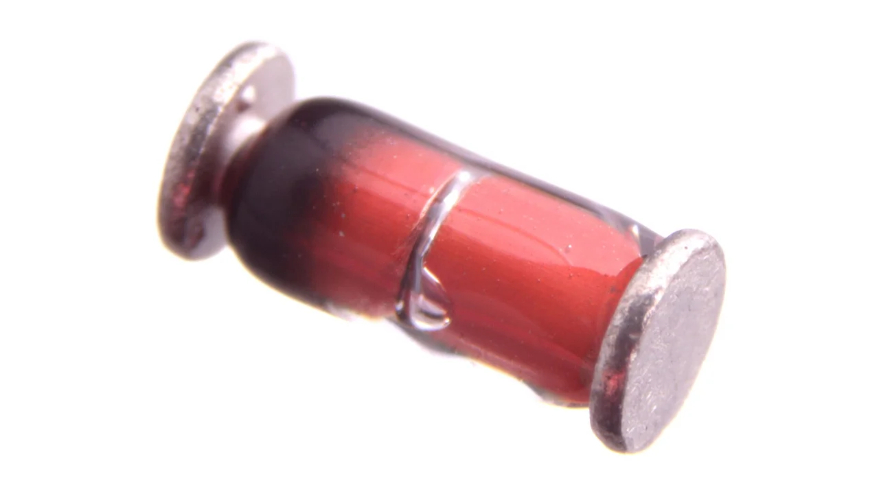
MiniMELF (SOD-80, DO-213AA) Component Package MiniMELF is a cylindrical, 2-lead SMD component package. It is a hermetically sealed glass-based package, which offers components with superb reliability characteristics. Like it's larger MELF cousin, they are a pain to solder because they roll around!
MiniMELF (SOD-80, DO-213AA) Component Package MiniMELF is a cylindrical, 2-lead SMD component package. It is a hermetically sealed glass-based package, which offers components with superb reliability characteristics. Like it's larger MELF cousin, they are a pain to solder because they roll around!
MLP is a synonym for the QFN component package used by Fairchild Semiconductor.
MLP Component Package MLP is a synonym for the QFN component package used by Fairchild Semiconductor.
MPAK is the package code used by NXP Semiconductors for the SOT-23-3 component package.
MPAK Component Package MPAK is the package code used by NXP Semiconductors for the SOT-23-3 component package.
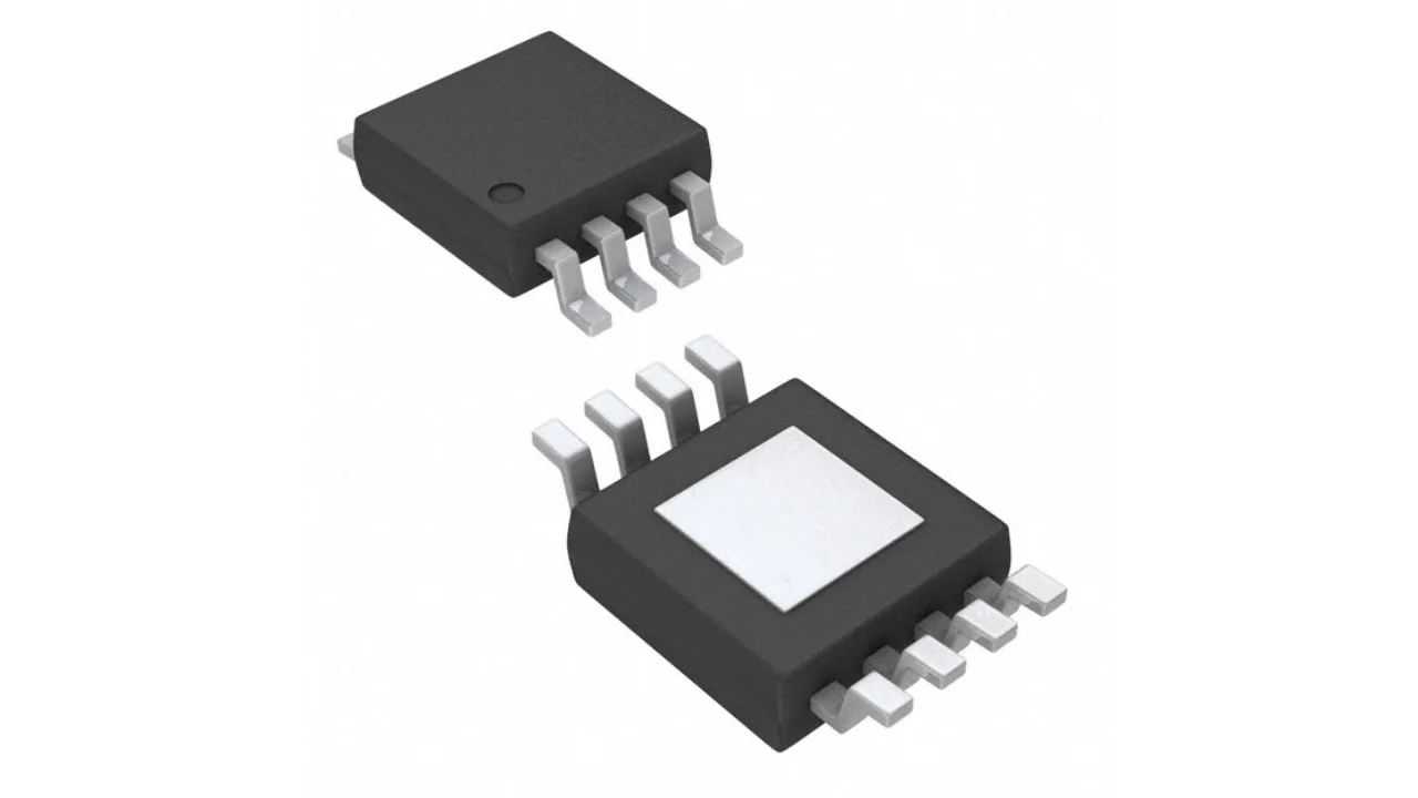
MSOP is a family of SMD component packages with gull-wing leads. It is a miniaturized version of the SSOP package.
MSOP Component Package MSOP is a family of SMD component packages with gull-wing leads. It is a miniaturized version of the SSOP package.
PDIP is a variant of the DIP package that uses plastic for the enclosure.
PDIP Component Package PDIP is a variant of the DIP package that uses plastic for the enclosure.
PDMU is a synonym for the SOD-123F used by Rohm Semiconductor, the flat-lead variant of the SOD-123 package family.
PDMU Component Package PDMU is a synonym for the SOD-123F used by Rohm Semiconductor, the flat-lead variant of the SOD-123 package family.
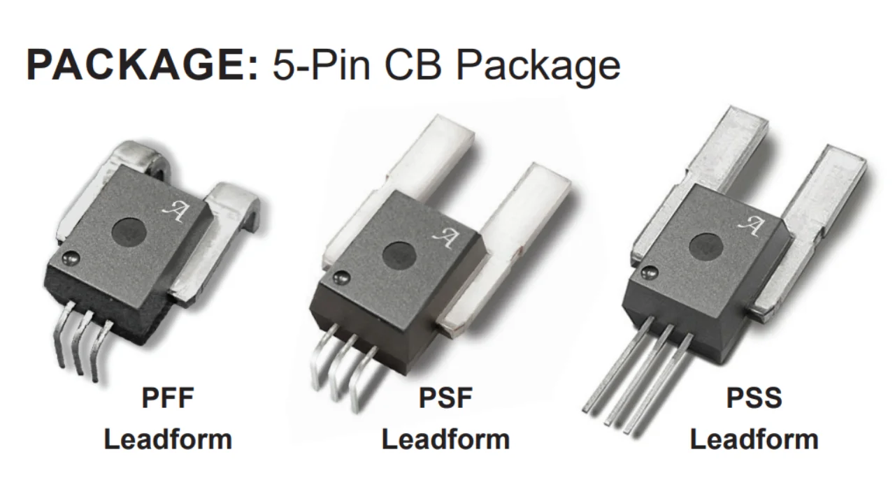
PFF, PSF and PSS Leadform Component Packages PFF, PSF and PSS are Allegro MicroSystems package names used for certain through-hole integrated current sensors.
PFF, PSF and PSS Leadform Component Packages PFF, PSF and PSS are Allegro MicroSystems package names used for certain through-hole integrated current sensors.
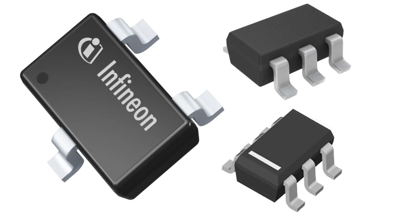
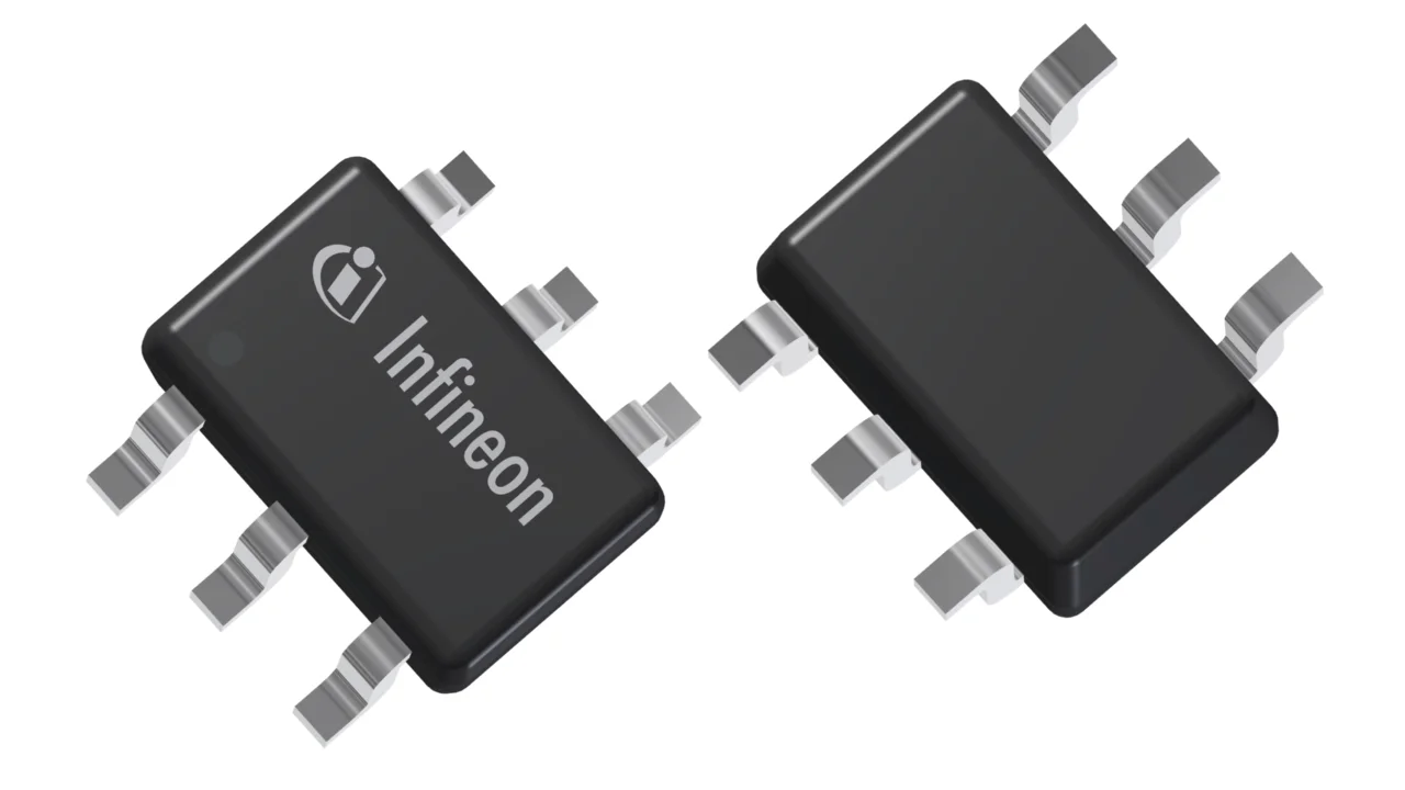
PG-SCT595 Component Package PG-SCT595 is a 5-lead gull-wing SMD component package used by Infineon.
PG-SCT595 Component Package PG-SCT595 is a 5-lead gull-wing SMD component package used by Infineon.
PLCC is a variant within the chip carrier package family.
PLCC Component Package PLCC is a variant within the chip carrier package family.
PowerDI123 Component Package Variants, pin counts, pitches, solderability, thermal resistances, dimensions, land patterns, 3D models and more info for the PowerDI123 component package.
PowerDI123 Component Package Variants, pin counts, pitches, solderability, thermal resistances, dimensions, land patterns, 3D models and more info for the PowerDI123 component package.
PowerPAK SO-8 Component Package
PowerPAK SO-8 Component Package
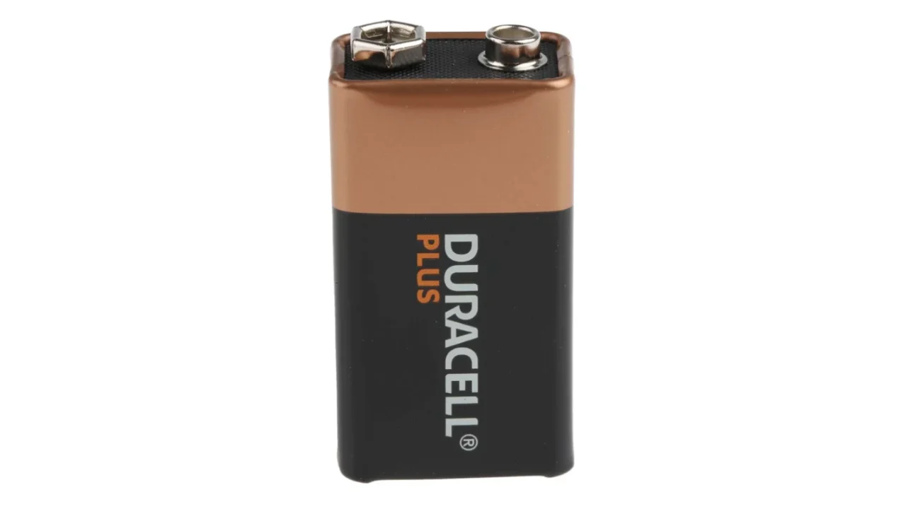
PP3 is the name for the most common 9V battery size.
PP3 Component Package PP3 is the name for the most common 9V battery size.
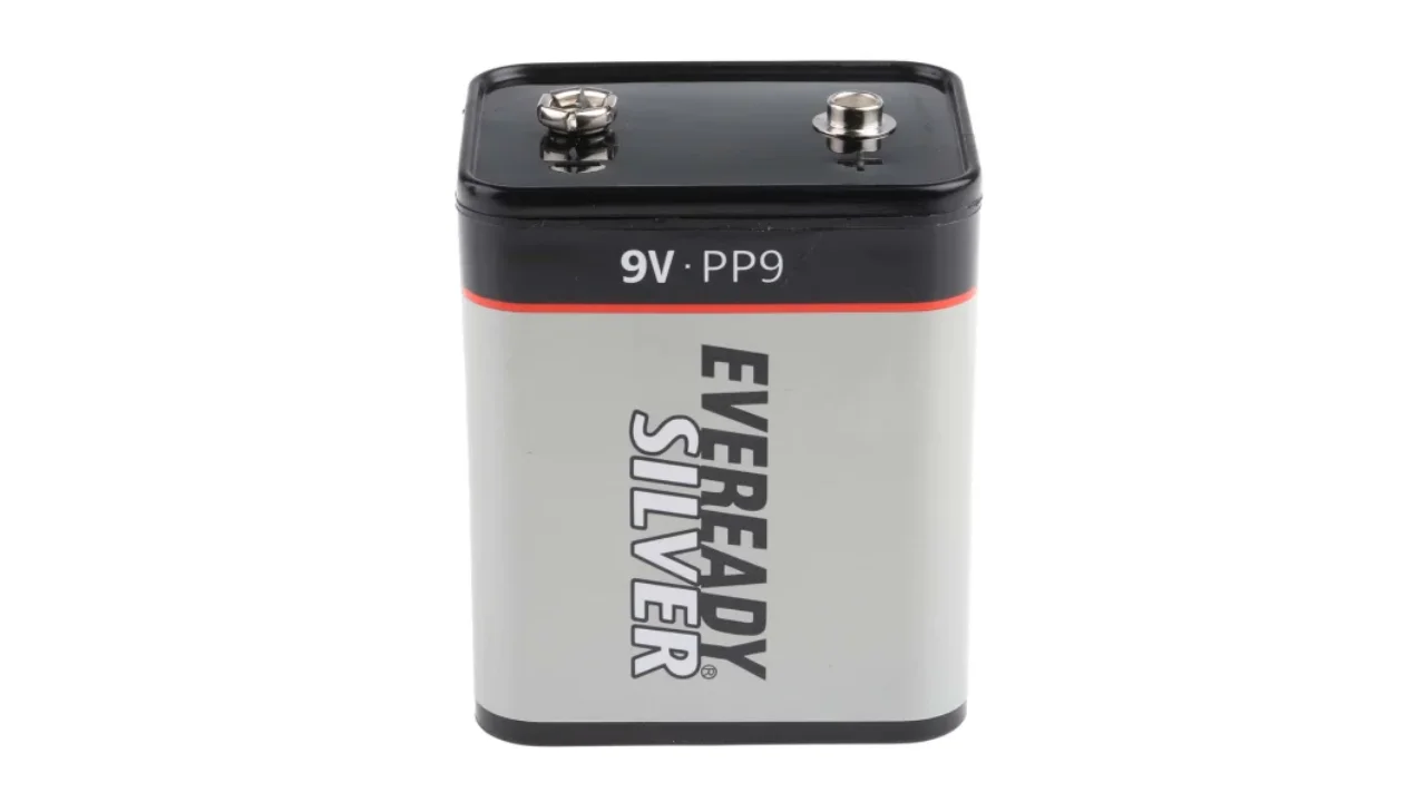
PP9 is a less common 9V battery component package that is similar to the common PP3 package.
PP9 Component Package PP9 is a less common 9V battery component package that is similar to the common PP3 package.
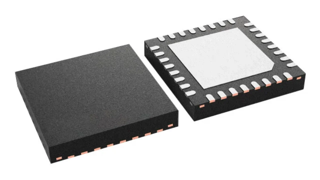
QFN is a family of SMD packages with pads around all four sides, plus an optional thermal pad in the center. Along with QFP, it is commonly used for medium pin count ICs.
QFN Component Package QFN is a family of SMD packages with pads around all four sides, plus an optional thermal pad in the center. Along with QFP, it is commonly used for medium pin count ICs.
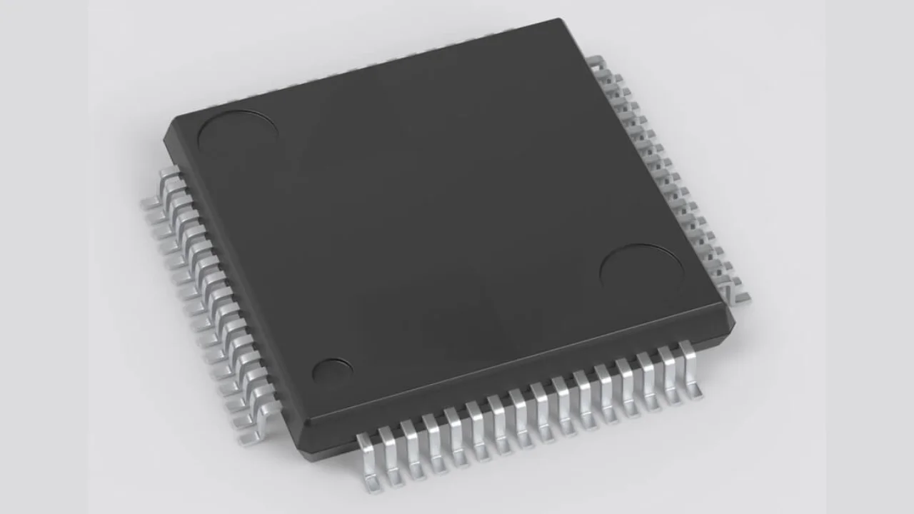
QFP is a family of SMD packages with gull-wing leads protruding from all four sides. It is commonly used for medium pin count ICs.
QFP Component Package QFP is a family of SMD packages with gull-wing leads protruding from all four sides. It is commonly used for medium pin count ICs.
QIP is an older through-hole component package with four rows of pins, rather than the more common two rows of pins found in the DIP package.
QIP Component Package QIP is an older through-hole component package with four rows of pins, rather than the more common two rows of pins found in the DIP package.
RT-3 is a package code used by Analog Devices for the SOT-23-3 component package.
RT-3 Component Package RT-3 is a package code used by Analog Devices for the SOT-23-3 component package.
SC-101 is a synonym (JEITA) for the SOT-883 component package.
SC-101 Component Package SC-101 is a synonym (JEITA) for the SOT-883 component package.
SC-104A Component Package SC-104A is a synonym (JEITA) for the SOD-723 component package.
SC-104A Component Package SC-104A is a synonym (JEITA) for the SOD-723 component package.
SC-109D Component Package SC-109D is a synonym (JEITA) for the SOD-123 component package.
SC-109D Component Package SC-109D is a synonym (JEITA) for the SOD-123 component package.
SC-116A Component Package SC-116A is a synonym (JEITA) for the SOD-923 component package.
SC-116A Component Package SC-116A is a synonym (JEITA) for the SOD-923 component package.
SC-59 is the JEITA EIAJ package code for the SOT-23-3 component package.
SC-59 Component Package SC-59 is the JEITA EIAJ package code for the SOT-23-3 component package.
SC-63 is the JEITA/EIAJ name for the TO-252-3 component package.
SC-63 Component Package SC-63 is the JEITA/EIAJ name for the TO-252-3 component package.
SC-70 is a synonym (JEITA) for the SOT-323-3 (3-pin variant) of the SOT-323 family of component packages.
SC-70 Component Package SC-70 is a synonym (JEITA) for the SOT-323-3 (3-pin variant) of the SOT-323 family of component packages.
SC-70-5 Component Package SC-70-5 is a synonym (JEITA) for the SOT-353 component package.
SC-70-5 Component Package SC-70-5 is a synonym (JEITA) for the SOT-353 component package.
SC-74A is a synonym (JEITA) for a variant of the SOT-23 component package family.
SC-74A Component Package SC-74A is a synonym (JEITA) for a variant of the SOT-23 component package family.
SC-75 is a synonym (JEITA) for the SOT-416FL component package.
SC-75 Component Package SC-75 is a synonym (JEITA) for the SOT-416FL component package.
SC-76 is a synonym for the SOD-323 component package.
SC-76 Component Package SC-76 is a synonym for the SOD-323 component package.
SC-79 is a synonym for the SOD-523 component package.
SC-79 Component Package SC-79 is a synonym for the SOD-523 component package.
SC-88A is a synonym for the SOT-353 component package.
SC-88A Component Package SC-88A is a synonym for the SOT-353 component package.
SC-89 can refer to the SC-89-3 (synonym for the SOT-490 component package) or the SC-89-6 (synonym for the SOT-563 component package).
SC-89 Component Package SC-89 can refer to the SC-89-3 (synonym for the SOT-490 component package) or the SC-89-6 (synonym for the SOT-563 component package).
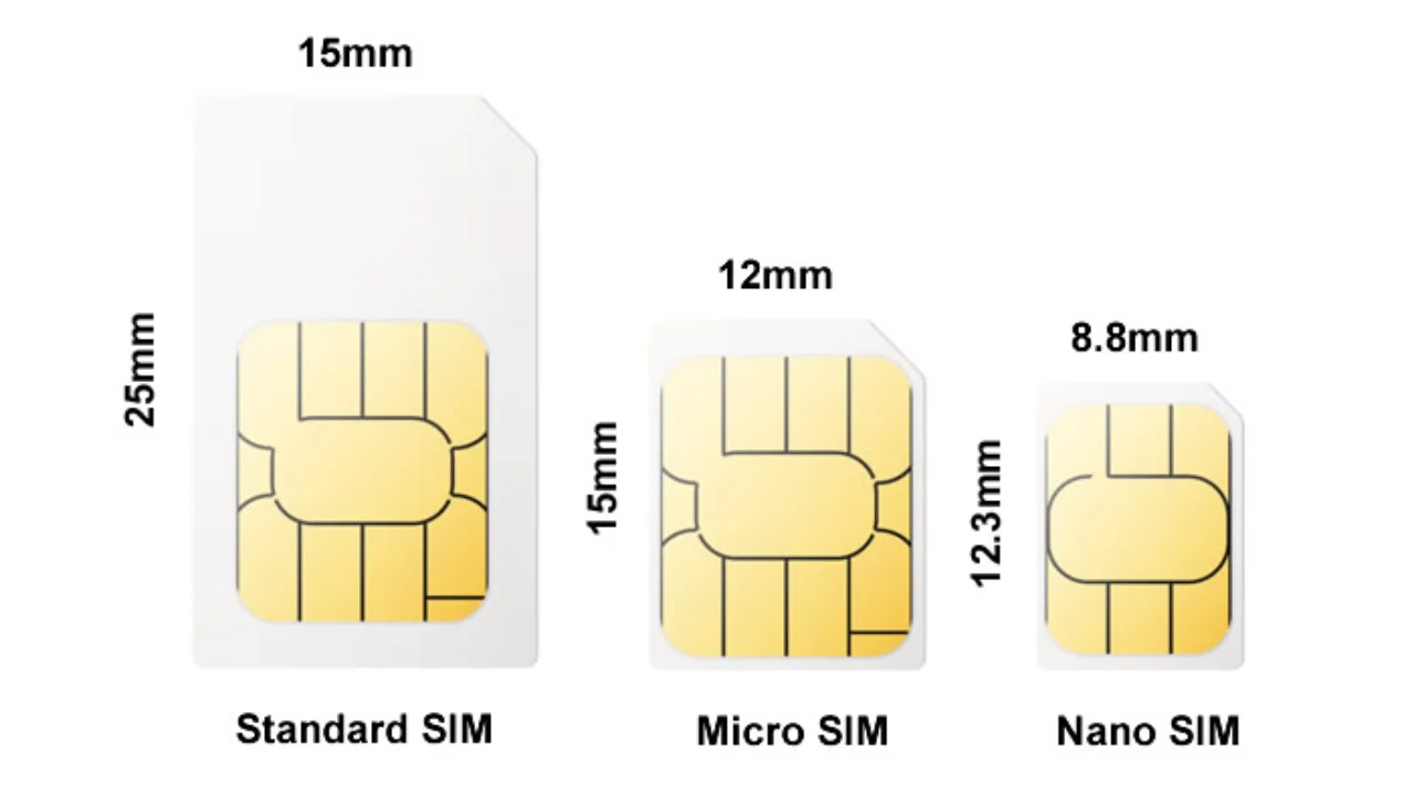
There a four standard SIM card sizes.
SIM Card Sizes There a four standard SIM card sizes.
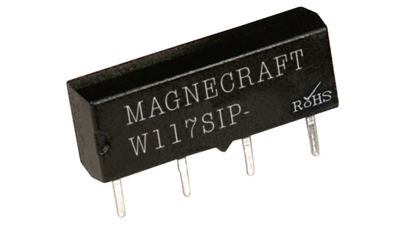
SIP is a older through-hole component package with a single row of 2.54mm pitch pins. It was/is commonly used for resistor networks and RAM chips.
SIP Component Package SIP is a older through-hole component package with a single row of 2.54mm pitch pins. It was/is commonly used for resistor networks and RAM chips.
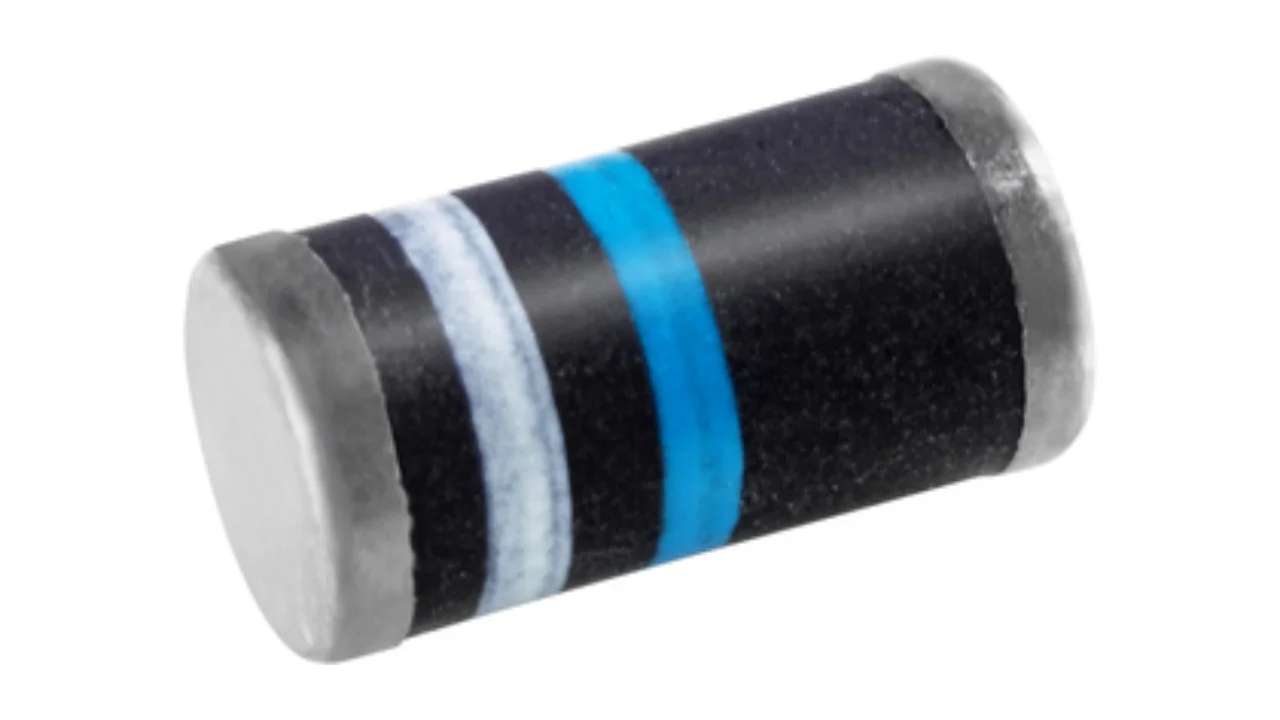
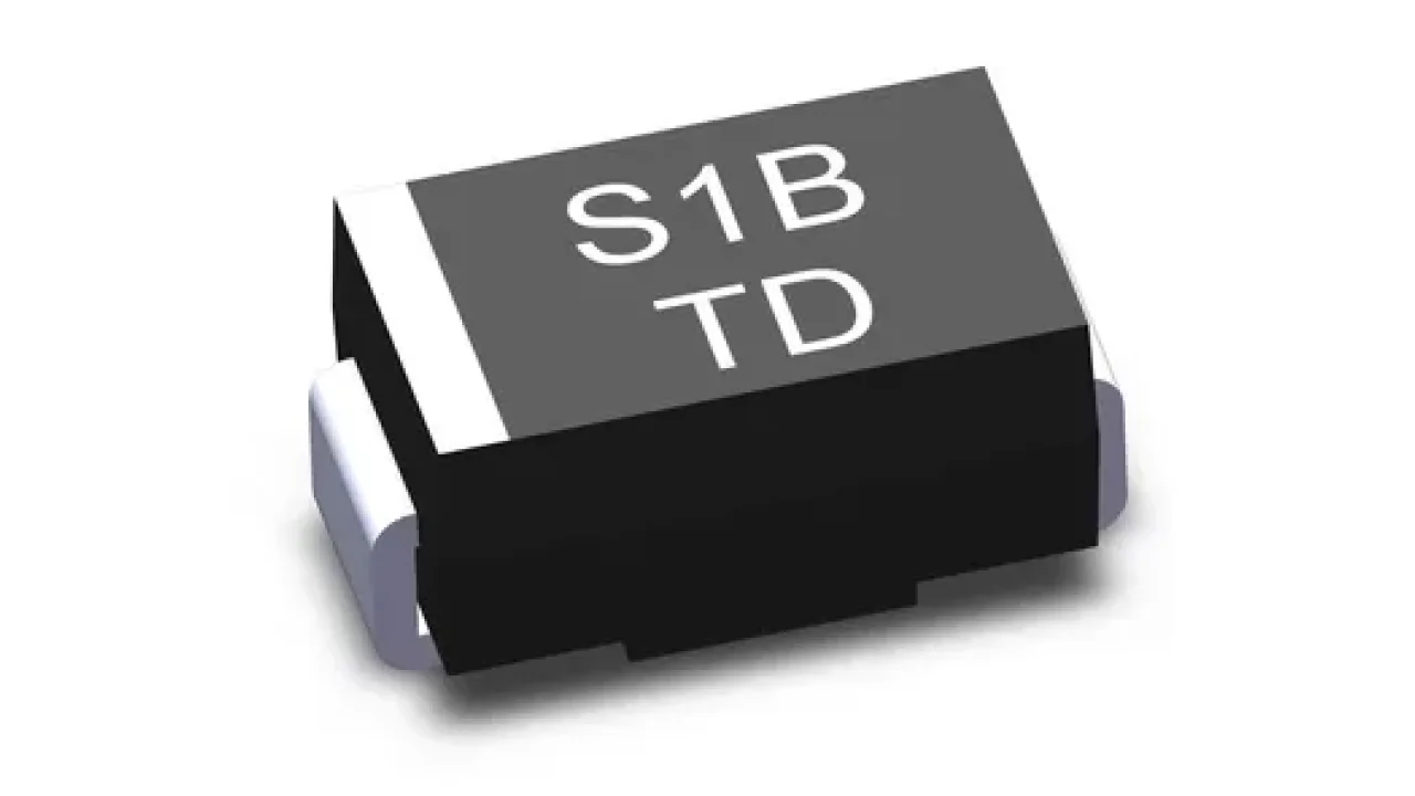
SMA (DO-214AC) Component Package SMA (DO-214AC) is a 2-lead SMD component package commonly used for diodes. SMA is the smallest package in the family containing SMA, SMB and SMC.
SMA (DO-214AC) Component Package SMA (DO-214AC) is a 2-lead SMD component package commonly used for diodes. SMA is the smallest package in the family containing SMA, SMB and SMC.
SMB (DO-214AA) Component Package SMB (DO-214AA) is a 2-lead SMD component package commonly used for diodes. It is in the same family as SMA (DO-214AC) and SMC (DO-214AB).
SMB (DO-214AA) Component Package SMB (DO-214AA) is a 2-lead SMD component package commonly used for diodes. It is in the same family as SMA (DO-214AC) and SMC (DO-214AB).
SMC (DO-214AB) Component Package SMC (DO-214AB) is a 2-lead SMD component package commonly used for diodes. It is the largest package in the family containing SMA, SMB and SMC.
SMC (DO-214AB) Component Package SMC (DO-214AB) is a 2-lead SMD component package commonly used for diodes. It is the largest package in the family containing SMA, SMB and SMC.
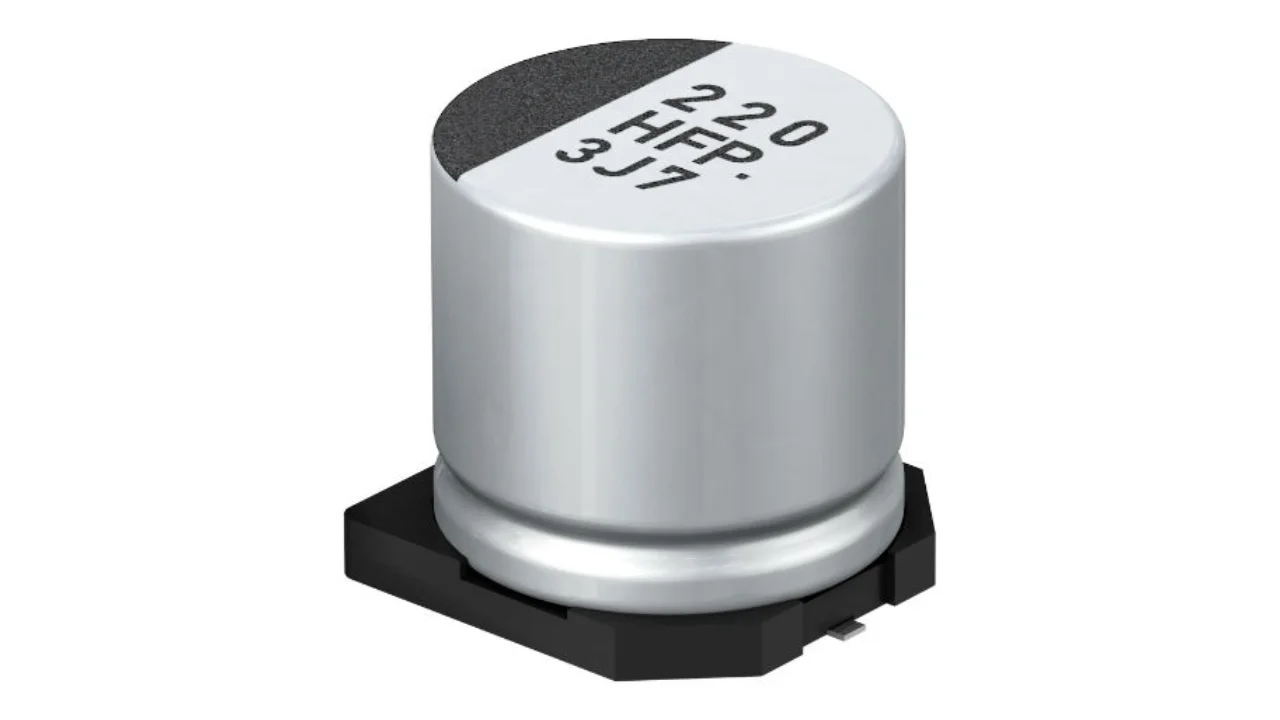
SMD Electrolytic Capacitor Packages SMD electrolytic capacitors come in a variety of industry standard packages.
SMD Electrolytic Capacitor Packages SMD electrolytic capacitors come in a variety of industry standard packages.
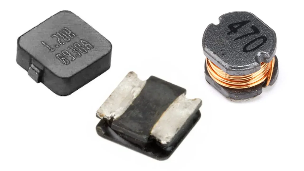
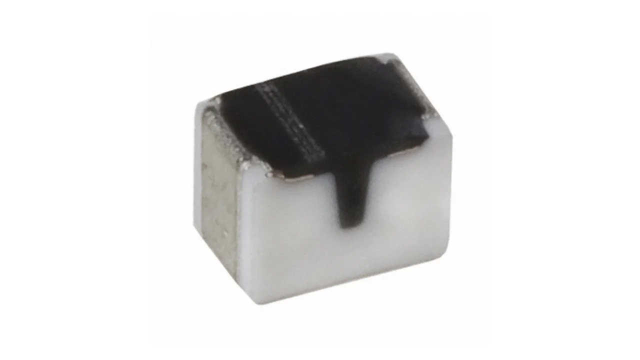
SMD inductors come in a variety of packages, but are not as standardized as other SMD components.
SMD Inductor Packages SMD inductors come in a variety of packages, but are not as standardized as other SMD components.
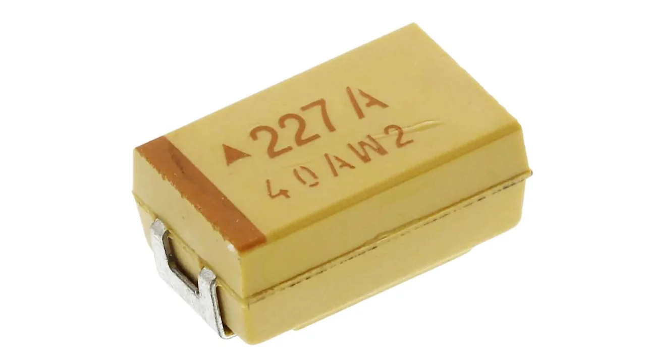
SMD Tantalum Capacitor Packages SMD tantalum capacitors are generally packaged in yellow or orange rectangular packages with two leads.
SMD Tantalum Capacitor Packages SMD tantalum capacitors are generally packaged in yellow or orange rectangular packages with two leads.
SMD-220 Component Package SMD-220 is a synonym for the TO-263 component package (because the TO-263 is considered to be the surface-mount equivalent of the TO-220 package).
SMD-220 Component Package SMD-220 is a synonym for the TO-263 component package (because the TO-263 is considered to be the surface-mount equivalent of the TO-220 package).
SMD35 is a 2-lead SMD package used exclusively by Seti for their range of Deep UV LEDs.
SMD35 Component Package SMD35 is a 2-lead SMD package used exclusively by Seti for their range of Deep UV LEDs.
SMF (DO-219AB) is a 2-lead SMD package commonly used for diodes.
SMF Component Package SMF (DO-219AB) is a 2-lead SMD package commonly used for diodes.
SMT3 is a alias for the SOT-23-3 package used by NXP Semiconductors and Rohm Semiconductor.
SMT3 Component Package SMT3 is a alias for the SOT-23-3 package used by NXP Semiconductors and Rohm Semiconductor.
SNAPHAT Component Package SNAPHAT is a 28 or 44-pin SMD package used by ST Microelectronics for their range of battery-powered RTC modules. The top part containing the batteries and crystal can 'snap' into package after reflow, to avoid damaging the battery.
SNAPHAT Component Package SNAPHAT is a 28 or 44-pin SMD package used by ST Microelectronics for their range of battery-powered RTC modules. The top part containing the batteries and crystal can 'snap' into package after reflow, to avoid damaging the battery.
SOD-106 Component Package SOD-106 is a synonym for the MELF package.
SOD-106 Component Package SOD-106 is a synonym for the MELF package.
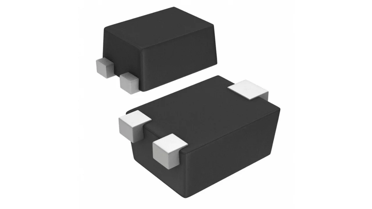
SOD-110 Component Package SOD-110 is a small 2-lead SMD package used for diodes.
SOD-110 Component Package SOD-110 is a small 2-lead SMD package used for diodes.
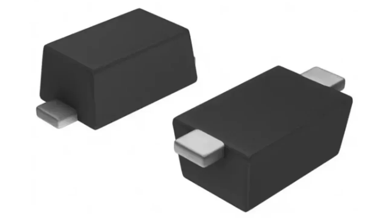
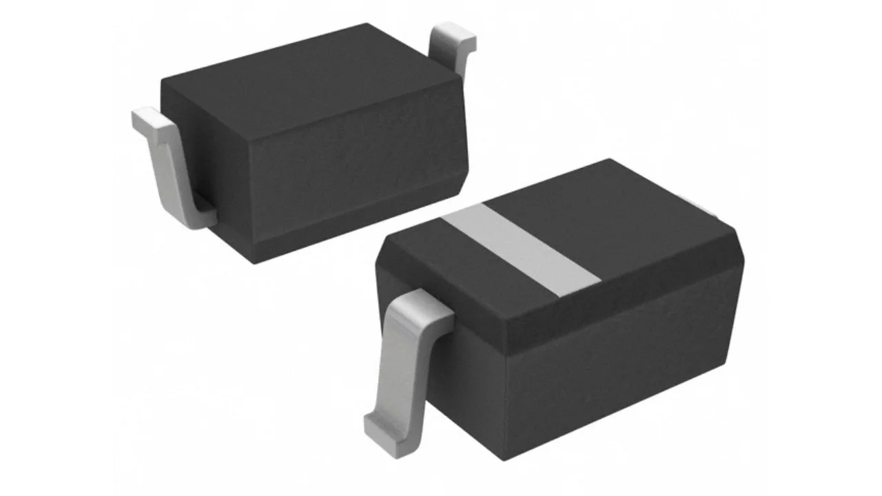
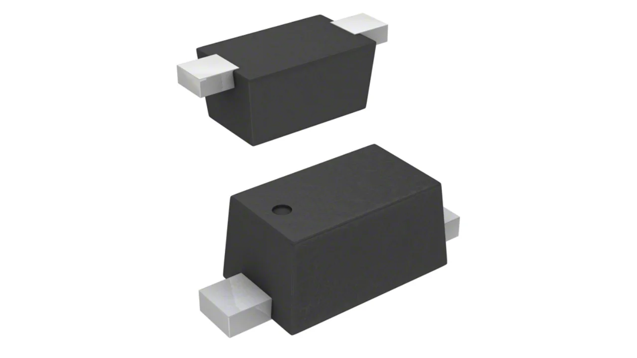
SOD-123 Component Package SOD-123 is a family of medium-sized SMD component packages with gull-wing leads. It is related to the SOD-323, SOD-523, SOD-723 and SOD-923 packages. It is commonly used for diodes.
SOD-123 Component Package SOD-123 is a family of medium-sized SMD component packages with gull-wing leads. It is related to the SOD-323, SOD-523, SOD-723 and SOD-923 packages. It is commonly used for diodes.
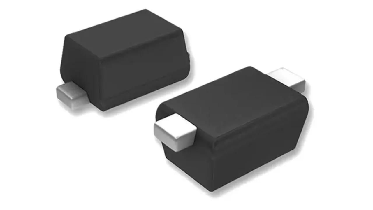
SOD-123F Component Package SOD-123F is a variant of the SOD-123 package with flat leads.
SOD-123F Component Package SOD-123F is a variant of the SOD-123 package with flat leads.
SOD-128 Component Package SOD-128 is a 2 flat lead SMD component package used by a few manufacturers for diodes.
SOD-128 Component Package SOD-128 is a 2 flat lead SMD component package used by a few manufacturers for diodes.
SOD-27 is a NXP synonym for the DO-34 package, a hermetically sealed, 2 lead glass TH package used for diodes.
SOD-27 Component Package SOD-27 is a NXP synonym for the DO-34 package, a hermetically sealed, 2 lead glass TH package used for diodes.
SOD-323 Component Package SOD-323 is a family of 2 lead SMD component packages, commonly used for diodes. It is related to the SOD-123, SOD-523, SOD-723 and SOD-923 packages.
SOD-323 Component Package SOD-323 is a family of 2 lead SMD component packages, commonly used for diodes. It is related to the SOD-123, SOD-523, SOD-723 and SOD-923 packages.
SOD-429 Component Package SOD-429 is a Nexperia synonym for the 3-lead variant of the TO-247AC package, the TO-247AC.
SOD-429 Component Package SOD-429 is a Nexperia synonym for the 3-lead variant of the TO-247AC package, the TO-247AC.
SOD-523 Component Package SOD-523 is a 2 lead SMD component package commonly used for diodes. It is related to the SOD-123, SOD-323, SOD-723 and SOD-923 packages.
SOD-523 Component Package SOD-523 is a 2 lead SMD component package commonly used for diodes. It is related to the SOD-123, SOD-323, SOD-723 and SOD-923 packages.
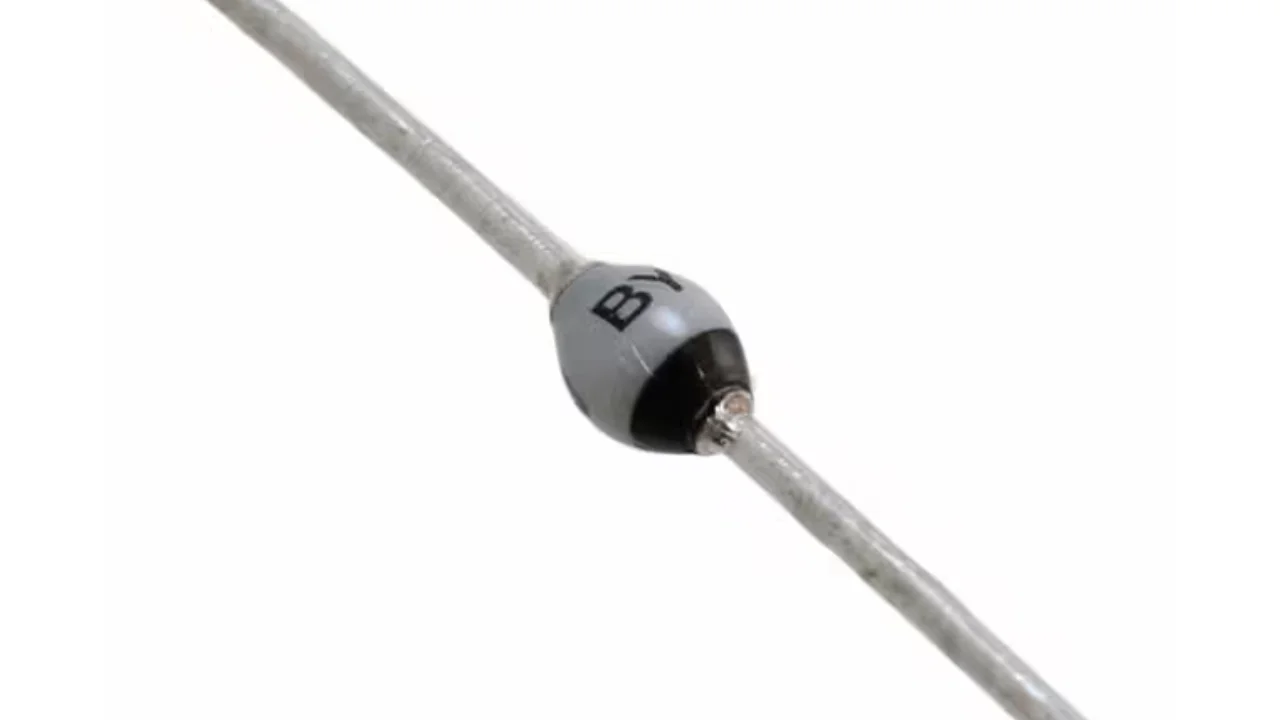
SOD-57 is a older glass passivated hermetically sealed 2-lead through-hole component package used for diodes that was somewhat popular in the late 1970s and 1980s.
SOD-57 Component Package SOD-57 is a older glass passivated hermetically sealed 2-lead through-hole component package used for diodes that was somewhat popular in the late 1970s and 1980s.
SOD-64 is a older glass passivated hermetically sealed 2-lead through-hole component package used for diodes that was somewhat popular in the late 1970s and 1980s.
SOD-64 Component Package SOD-64 is a older glass passivated hermetically sealed 2-lead through-hole component package used for diodes that was somewhat popular in the late 1970s and 1980s.
SOD-66 is a Nexperia synonym for the DO-41/DO-204AL package.
SOD-66 Component Package SOD-66 is a Nexperia synonym for the DO-41/DO-204AL package.
SOD-723 (SC-104A) Component Package SOD-723 is a 2-lead SMD package used for diodes.
SOD-723 (SC-104A) Component Package SOD-723 is a 2-lead SMD package used for diodes.
SOD-80 is a synonym for the MiniMELF package.
SOD-80 Component Package SOD-80 is a synonym for the MiniMELF package.
SOD-882 Component Package SOD-882 is a 2-lead SMD package used for diodes.
SOD-882 Component Package SOD-882 is a 2-lead SMD package used for diodes.
SOD-923 Component Package SOD-923 is a family of 2-lead SMD packages used for diodes. It is the smallest in the family that includes SOD-123, SOD-323, SOD-523, SOD-723, and SOD-923.
SOD-923 Component Package SOD-923 is a family of 2-lead SMD packages used for diodes. It is the smallest in the family that includes SOD-123, SOD-323, SOD-523, SOD-723, and SOD-923.
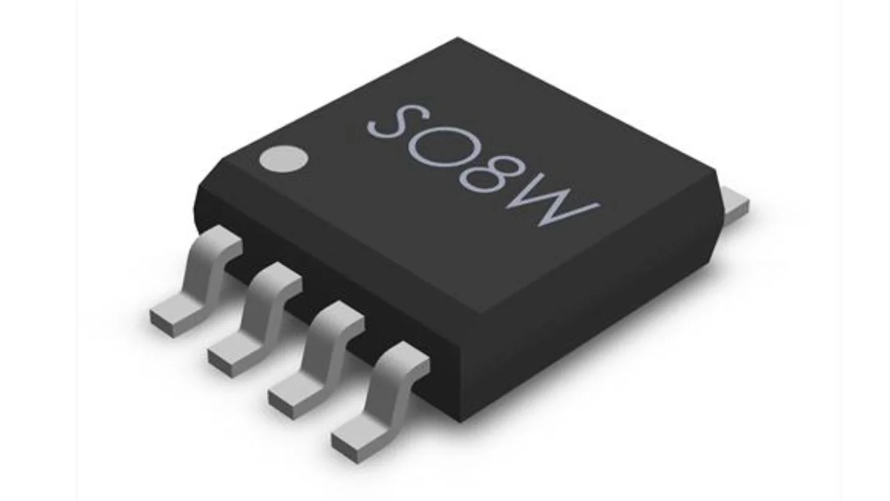
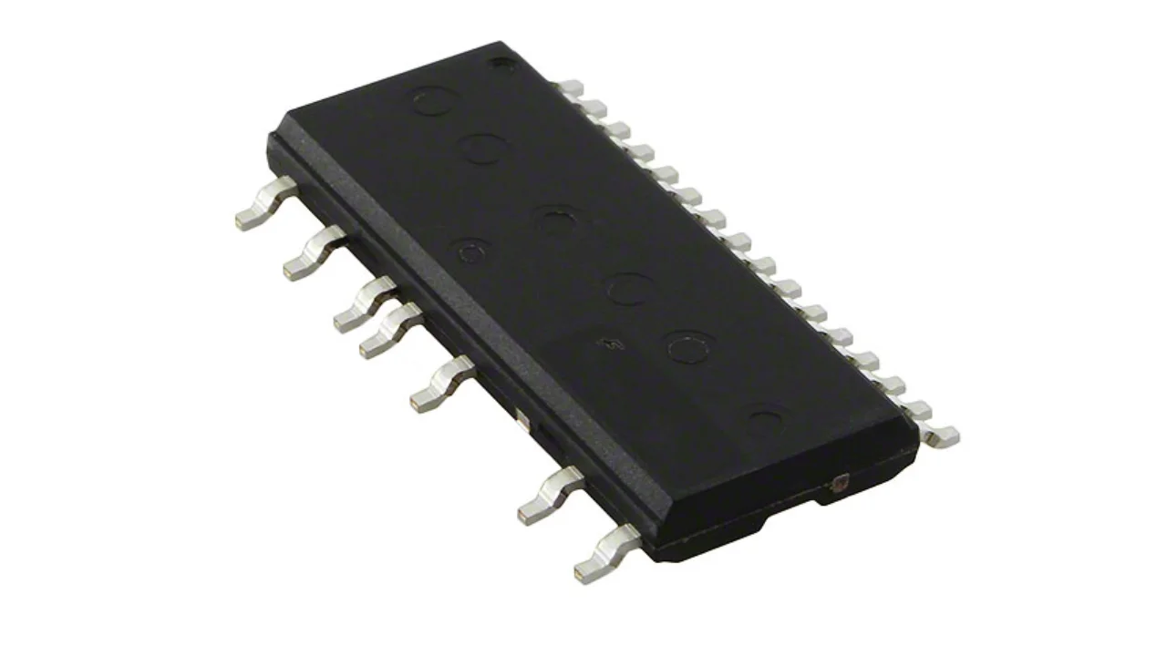
SOIC is a family of larger pitch SMD component packages that have gull-wing leads on two sides. There are three different widths of SOIC packages.
SOIC Component Package SOIC is a family of larger pitch SMD component packages that have gull-wing leads on two sides. There are three different widths of SOIC packages.
SOJ is a family of SMD component packages with J-type leads on two sides. It is commonly used to house ICs. It is related to the PLCC package which has J-type leads on all four sides.
SOJ Component Package SOJ is a family of SMD component packages with J-type leads on two sides. It is commonly used to house ICs. It is related to the PLCC package which has J-type leads on all four sides.
SON is a synonym for the DFN component package.
SON Component Package SON is a synonym for the DFN component package.
SOP is a family of SMD component packages with gull-wing leads on two sides.
SOP Component Package SOP is a family of SMD component packages with gull-wing leads on two sides.
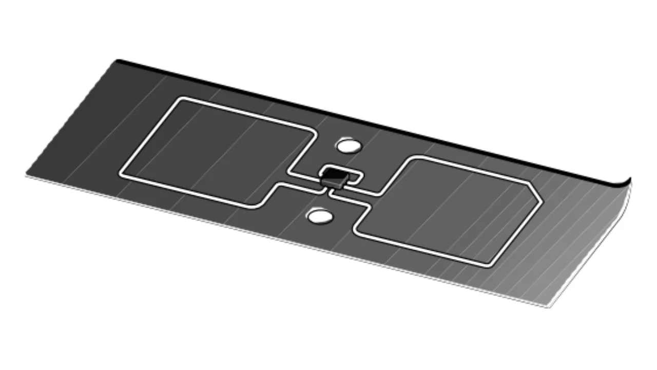
SOT-1040-1 Component Package SOT-1040-1 is a component package exclusively used by NXP for some of their RFID inlays.
SOT-1040-1 Component Package SOT-1040-1 is a component package exclusively used by NXP for some of their RFID inlays.
SOT-106A Component Package SOT-106A is a synonym for the TO-220F variant in the TO-220 family.
SOT-106A Component Package SOT-106A is a synonym for the TO-220F variant in the TO-220 family.
SOT-1193 Component Package SOT-1193 is a SMD component package used for NXP RFID ICs.
SOT-1193 Component Package SOT-1193 is a SMD component package used for NXP RFID ICs.
SOT-1210 Component Package SOT-1210 is a synonym for the LFPAK33 component package.
SOT-1210 Component Package SOT-1210 is a synonym for the LFPAK33 component package.
SOT-1226-2 Component Package SOT-1226-2 is a SMD component package used by NXP with 8 leads and a pitch of 0.5mm.
SOT-1226-2 Component Package SOT-1226-2 is a SMD component package used by NXP with 8 leads and a pitch of 0.5mm.
SOT-1235 Component Package SOT-1235 is a synonym for the LFPAK88 component package.
SOT-1235 Component Package SOT-1235 is a synonym for the LFPAK88 component package.
SOT-143 Component Package SOT-143 is a 4 gull-wing lead SMD package which is easily distinguishable by having one wider lead compared with the other 3.
SOT-143 Component Package SOT-143 is a 4 gull-wing lead SMD package which is easily distinguishable by having one wider lead compared with the other 3.
SOT-1571-1 Component Package SOT-1571-1 is a package code used by NXP for a QFP, 48pin, 7x7x1.4mm body, 0.5mm pitch, 4.5x4.5mm EP component package.
SOT-1571-1 Component Package SOT-1571-1 is a package code used by NXP for a QFP, 48pin, 7x7x1.4mm body, 0.5mm pitch, 4.5x4.5mm EP component package.
SOT-162-1 Component Package SOT-162-1 is a NXP synonym for the SOIC-16W component package.
SOT-162-1 Component Package SOT-162-1 is a NXP synonym for the SOIC-16W component package.
SOT-223 Component Package SOT-223 is a family of SMD component packages with gull-wing leads on one side and a tab on the other side. It is commonly used for medium-power discrete semiconductor components and basic ICs such as linear regulators.
SOT-223 Component Package SOT-223 is a family of SMD component packages with gull-wing leads on one side and a tab on the other side. It is commonly used for medium-power discrete semiconductor components and basic ICs such as linear regulators.
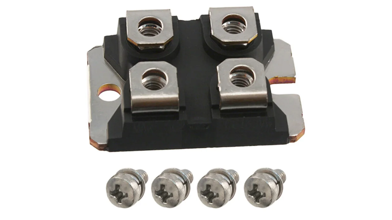
SOT-227 Component Package SOT-227 is a high-power package with M4 screw terminals. It is used by companies such as Vishay and IXYS for high-voltage and high-current diodes.
SOT-227 Component Package SOT-227 is a high-power package with M4 screw terminals. It is used by companies such as Vishay and IXYS for high-voltage and high-current diodes.
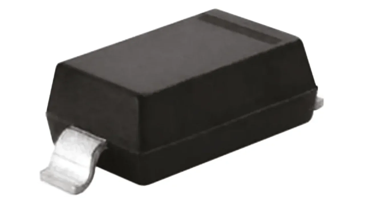
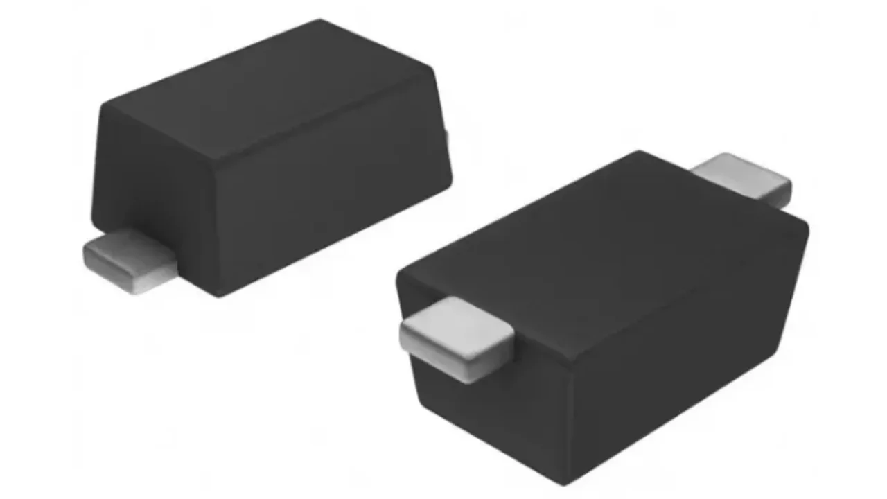
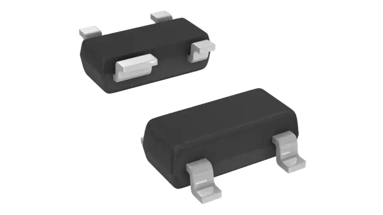
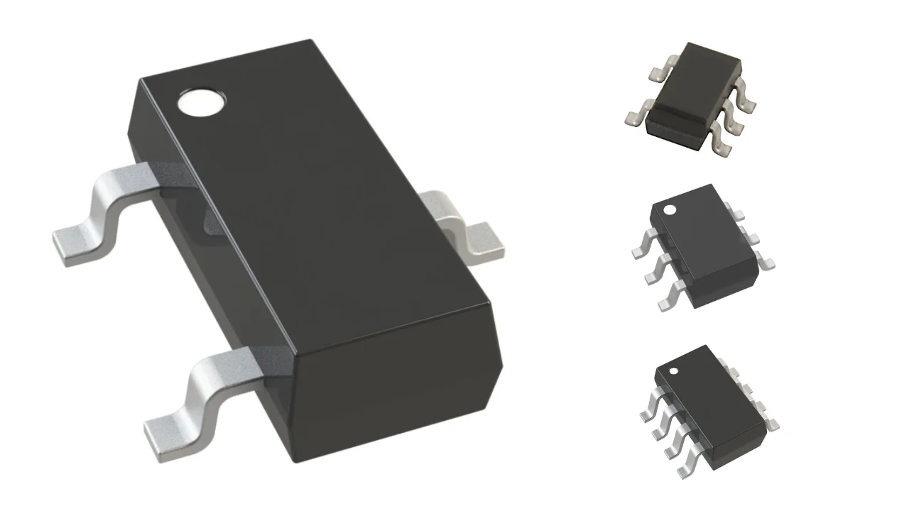
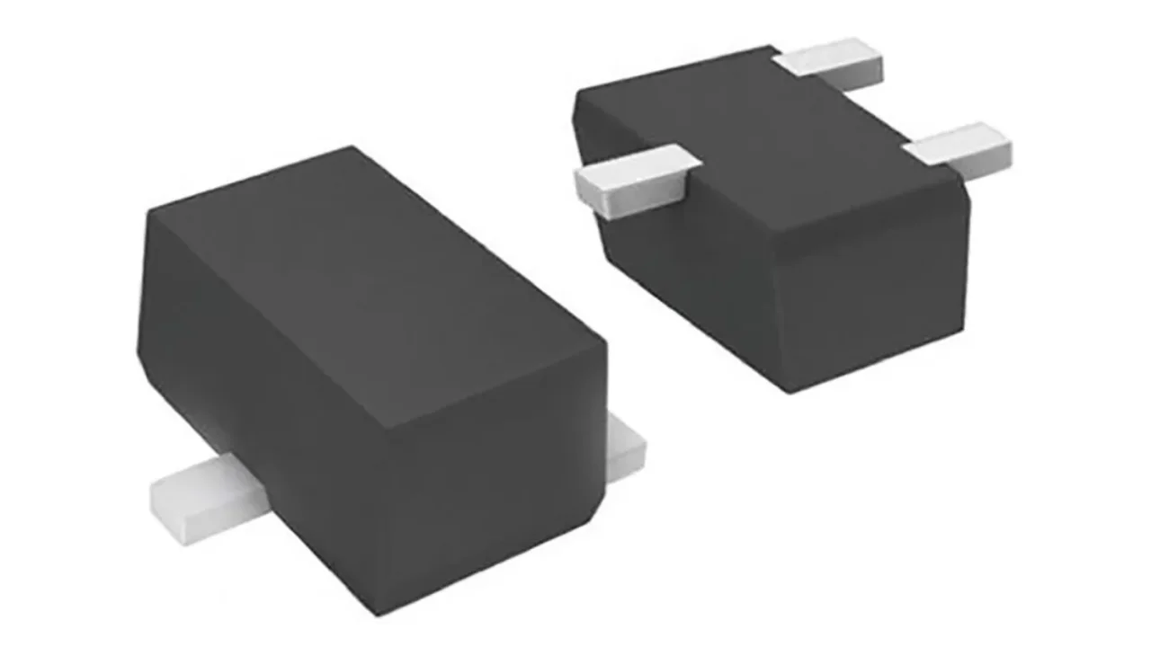
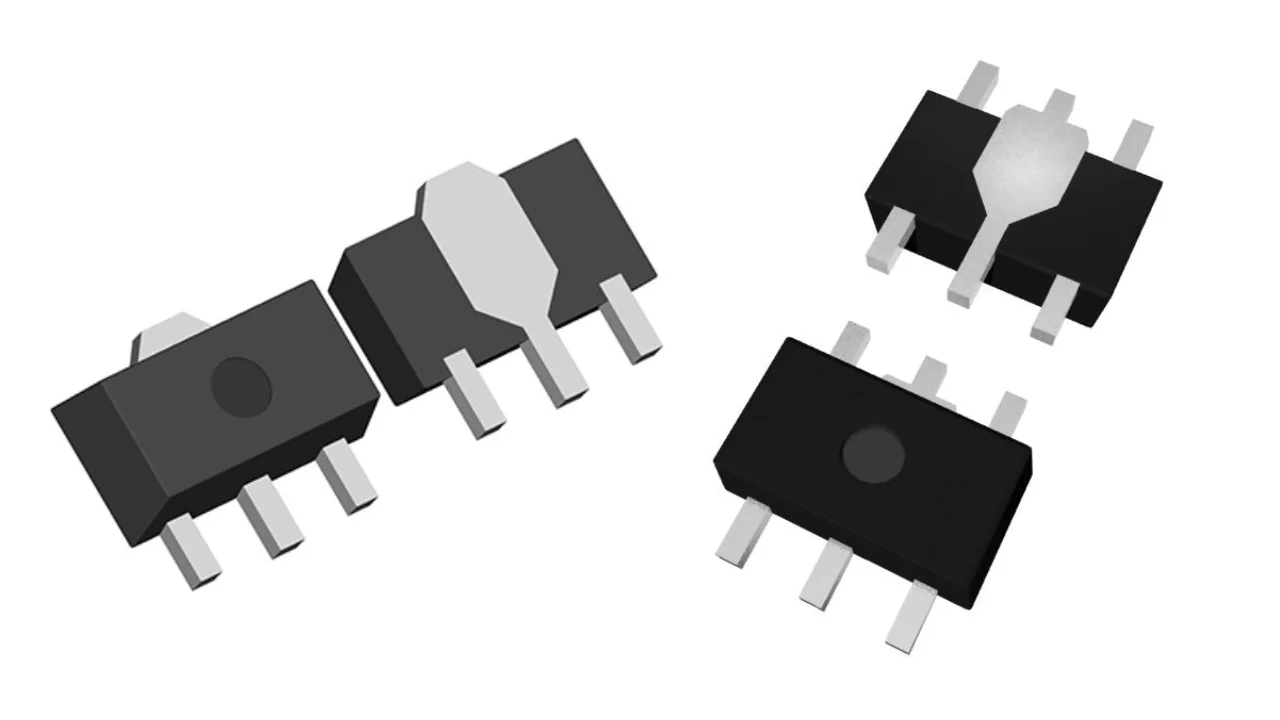
SOT-23 is a popular medium-sized SMD package with 3 to 8 gull-wing leads. It is used for a wide range of devices such as linear regulators, BJTs, MOSFETs and diodes.
SOT-23 Component Package SOT-23 is a popular medium-sized SMD package with 3 to 8 gull-wing leads. It is used for a wide range of devices such as linear regulators, BJTs, MOSFETs and diodes.
SOT-23F Component Package SOT-23F is a 3-pin SMD component package that is very similar to the SOT-23 package, except the leads are flat rather than gull-wing.
SOT-23F Component Package SOT-23F is a 3-pin SMD component package that is very similar to the SOT-23 package, except the leads are flat rather than gull-wing.
SOT-323 Component Package SOT-323 is a family of SMD component packages with gull-wing leads on two sides. The most popular variant is the SOT-323-3 (SC-70-3) which is commonly used for transistors.
SOT-323 Component Package SOT-323 is a family of SMD component packages with gull-wing leads on two sides. The most popular variant is the SOT-323-3 (SC-70-3) which is commonly used for transistors.
SOT-346 Component Package SOT-346 is a synonym of the SOT-23-3 package.
SOT-346 Component Package SOT-346 is a synonym of the SOT-23-3 package.
SOT-353 Component Package SOT-353 is a 5 gull-wing lead SMD component package with a pitch of 0.65mm.
SOT-353 Component Package SOT-353 is a 5 gull-wing lead SMD component package with a pitch of 0.65mm.
SOT-363 (SC-88) Component Package SOT-363 (SC-88, TSSOP6) is a SMD component package with gull-wing leads on two sides.
SOT-363 (SC-88) Component Package SOT-363 (SC-88, TSSOP6) is a SMD component package with gull-wing leads on two sides.
SOT-416 Component Package SOT-416 is a family of 3-lead SMD component packages. There are two variants, SOT-416 (gull-wing leads) and SOT-416FL (flat leads).
SOT-416 Component Package SOT-416 is a family of 3-lead SMD component packages. There are two variants, SOT-416 (gull-wing leads) and SOT-416FL (flat leads).
SOT-428 Component Package SOT-428 is a popular synonym for the TO-252-3 component package (3-lead variant of the TO-252 family).
SOT-428 Component Package SOT-428 is a popular synonym for the TO-252-3 component package (3-lead variant of the TO-252 family).
SOT-457 Component Package SOT-457 is a JEDEC name for the SOT-23-6 component package.
SOT-457 Component Package SOT-457 is a JEDEC name for the SOT-23-6 component package.
SOT-490 Component Package SOT-490 is a 3-lead SMD component package primarily used for transistors. It is similar to the SOT-416FL.
SOT-490 Component Package SOT-490 is a 3-lead SMD component package primarily used for transistors. It is similar to the SOT-416FL.
SOT-523F Component Package SOT-523F is a 3 gull-wing lead SMD component package.
SOT-523F Component Package SOT-523F is a 3 gull-wing lead SMD component package.
SOT-563 Component Package SOT-563 (SC-89-6) is a small 6 flat lead SMD component package.
SOT-563 Component Package SOT-563 (SC-89-6) is a small 6 flat lead SMD component package.
SOT-583 Component Package SOT-583 is an 8 flat lead SMD component package with a pitch of 0.5mm.
SOT-583 Component Package SOT-583 is an 8 flat lead SMD component package with a pitch of 0.5mm.
SOT-665 Component Package SOT-665 is a 5-lead SMD component package with a pitch of 0.5mm.
SOT-665 Component Package SOT-665 is a 5-lead SMD component package with a pitch of 0.5mm.
SOT-669 Component Package SOT-669 is a synonym for the LFPAK56 component package.
SOT-669 Component Package SOT-669 is a synonym for the LFPAK56 component package.
SOT-723 Component Package SOT-723 is a 3 flat lead SMD component package with a pitch of 0.8mm.
SOT-723 Component Package SOT-723 is a 3 flat lead SMD component package with a pitch of 0.8mm.
SOT-753 Component Package SOT-753 is a synonym for the SOT-23-5 component package.
SOT-753 Component Package SOT-753 is a synonym for the SOT-23-5 component package.
SOT-762-1 Component Package SOT-762-1 is a NXP synonym for a QFN-14 5x2 0.5mm pitch component package.
SOT-762-1 Component Package SOT-762-1 is a NXP synonym for a QFN-14 5x2 0.5mm pitch component package.
SOT-883 Component Package SOT-883 is a 3-lead SMD component package that is very similar to a DFN package.
SOT-883 Component Package SOT-883 is a 3-lead SMD component package that is very similar to a DFN package.
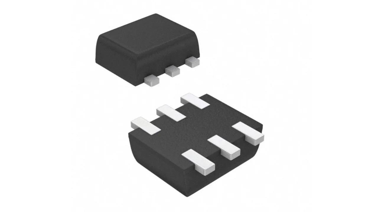
SOT-886 Component Package SOT-886 is a small 6-lead SMD component package commonly used for RFID tag chips, logic gates, buffer/line drivers and linear voltage regulators.
SOT-886 Component Package SOT-886 is a small 6-lead SMD component package commonly used for RFID tag chips, logic gates, buffer/line drivers and linear voltage regulators.
SOT-89 is a family to two small SMD component packages with gull-wing leads and a central tab-shaped lead. The SOT-89-3 and the SOT-89-5 are the two variants.
SOT-89 Component Package SOT-89 is a family to two small SMD component packages with gull-wing leads and a central tab-shaped lead. The SOT-89-3 and the SOT-89-5 are the two variants.
SOT-902 Component Package SOT-902 (MO-255) is a small family of SMD component packages with 8 leads.
SOT-902 Component Package SOT-902 (MO-255) is a small family of SMD component packages with 8 leads.
SOT-923 Component Package SOT-923 is a very small SMD component package.
SOT-923 Component Package SOT-923 is a very small SMD component package.
SOT-93 is a synonym for the TO-218-3 component package (3 pin variant of the TO-218 package).
SOT-93 Component Package SOT-93 is a synonym for the TO-218-3 component package (3 pin variant of the TO-218 package).
SPM23 is a proprietary Fairchild Semiconductor 23 gull-wing lead SMD component package which is used for some of their motor driver ICs.
SPM23 Component Package SPM23 is a proprietary Fairchild Semiconductor 23 gull-wing lead SMD component package which is used for some of their motor driver ICs.
SSOP is a family of SMD component packages with gull-wing leads. They can have both varying pitches and body widths.
SSOP Component Package SSOP is a family of SMD component packages with gull-wing leads. They can have both varying pitches and body widths.
SuperSOT-3 Component Package SuperSOT-3 is a package code used by Fairchild Semiconductor (now onsemi) for the SOT-23-3 (SOT-23 with 3 pins) package.
SuperSOT-3 Component Package SuperSOT-3 is a package code used by Fairchild Semiconductor (now onsemi) for the SOT-23-3 (SOT-23 with 3 pins) package.
Info on the TO-126 (TO-225AA, SOT-32) through-hole component package, including dimensions, thermal characteristics, heatsink mounting, and applications.
TO-126 Component Package Info on the TO-126 (TO-225AA, SOT-32) through-hole component package, including dimensions, thermal characteristics, heatsink mounting, and applications.
TO-18 is the TO-206AA variant of the TO-206 component package family.
TO-18 Component Package TO-18 is the TO-206AA variant of the TO-206 component package family.
TO-204 AA Component Package Variants, pin counts, pitches, solderability, thermal resistances, dimensions, land patterns, 3D models and more info for the TO-204 AA component package.
TO-204 AA Component Package Variants, pin counts, pitches, solderability, thermal resistances, dimensions, land patterns, 3D models and more info for the TO-204 AA component package.
TO-204 AD Component Package Variants, pin counts, pitches, solderability, thermal resistances, dimensions, land patterns, 3D models and more info for the TO-204 AD component package.
TO-204 AD Component Package Variants, pin counts, pitches, solderability, thermal resistances, dimensions, land patterns, 3D models and more info for the TO-204 AD component package.
TO-204 AE Component Package Variants, pin counts, pitches, solderability, thermal resistances, dimensions, land patterns, 3D models and more info for the TO-204 AE component package.
TO-204 AE Component Package Variants, pin counts, pitches, solderability, thermal resistances, dimensions, land patterns, 3D models and more info for the TO-204 AE component package.
TO-205AD Component Package TO-205AD is a synonym for the TO-39 component package.
TO-205AD Component Package TO-205AD is a synonym for the TO-39 component package.
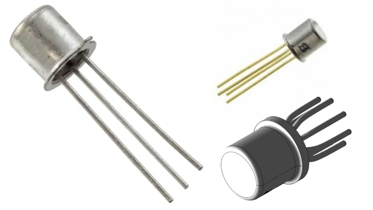
The TO-206 component package family is a family of large through-hole metal can packages used for things such as transistors, diodes and temperature sensors. There are variants with 2 to 8 leads. They are also known under the older names TO-18, TO-46 and TO-72.
TO-206 Component Package The TO-206 component package family is a family of large through-hole metal can packages used for things such as transistors, diodes and temperature sensors. There are variants with 2 to 8 leads. They are also known under the older names TO-18, TO-46 and TO-72.
TO-209AB Component Package TO-209AB is a synonym for the TO-93 component package.
TO-209AB Component Package TO-209AB is a synonym for the TO-93 component package.
The TO-218 component package family is a small family of through-hole packages commonly used for BJTs and MOSFETs. The most common variant is the TO-218-3 (3 lead variant).
TO-218 Component Package The TO-218 component package family is a small family of through-hole packages commonly used for BJTs and MOSFETs. The most common variant is the TO-218-3 (3 lead variant).
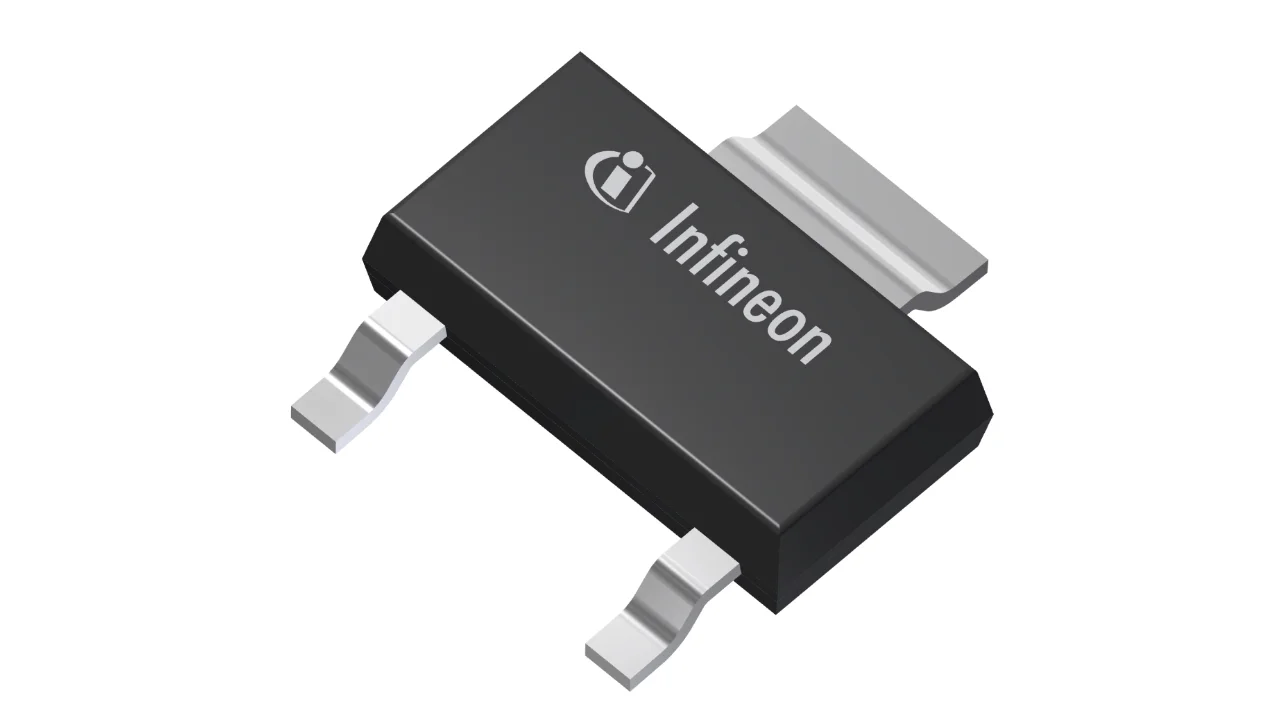
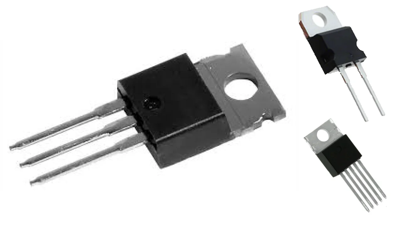
TO-220 is a popular family of through-hole component packages which are commonly used for power transistors, voltage regulators, and other power electronics components.
TO-220 Component Package TO-220 is a popular family of through-hole component packages which are commonly used for power transistors, voltage regulators, and other power electronics components.
TO-226 is a synonym for the TO-92 component package.
TO-226 Component Package TO-226 is a synonym for the TO-92 component package.
TO-23 is a through-hole transistor can component package. JEDEC transitioned the TO-23 designator to inactive in 1987. Very little information exists about this package online.
TO-23 Component Package TO-23 is a through-hole transistor can component package. JEDEC transitioned the TO-23 designator to inactive in 1987. Very little information exists about this package online.
TO-236AA Component Package TO-236AA is a synonym for the SOT-23-3, the 3-pin variant of the SOT-23 package.
TO-236AA Component Package TO-236AA is a synonym for the SOT-23-3, the 3-pin variant of the SOT-23 package.
TO-236AB Component Package TO-236AB is a synonym for the SOT-23-3, the 3-pin variant of the SOT-23 package.
TO-236AB Component Package TO-236AB is a synonym for the SOT-23-3, the 3-pin variant of the SOT-23 package.
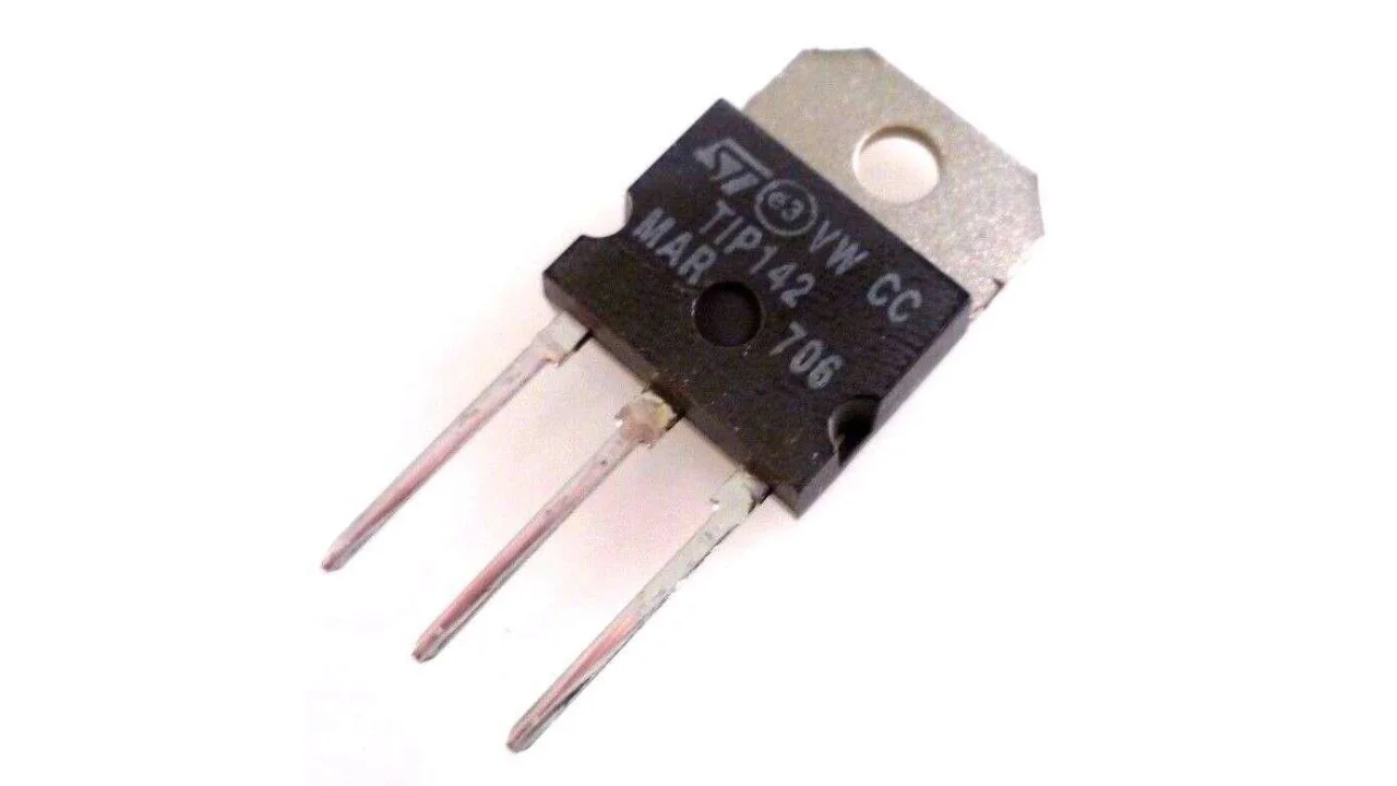
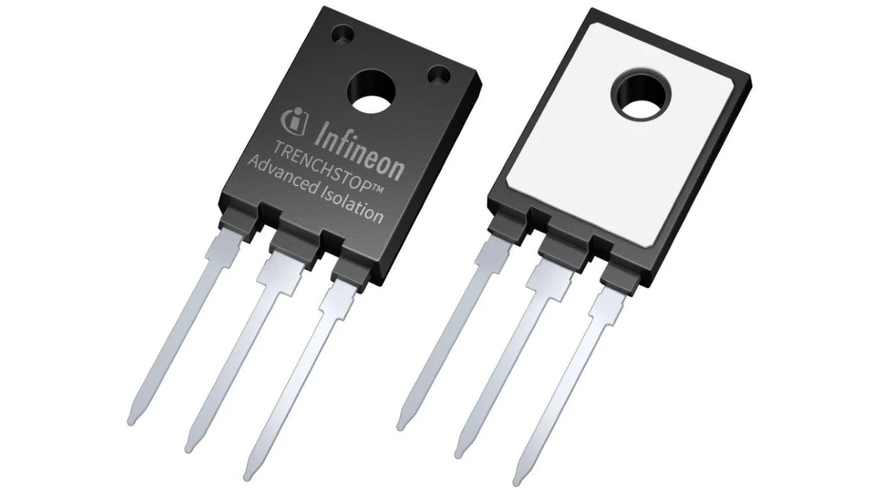
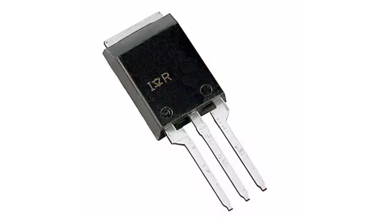
The TO-247 component package family is a family of large through-hole 3-leaded component packages commonly used for BJTs and MOSFETs. The most common variant is the TO-247AC (3 lead variant).
TO-247 Component Package The TO-247 component package family is a family of large through-hole 3-leaded component packages commonly used for BJTs and MOSFETs. The most common variant is the TO-247AC (3 lead variant).
TO-247AC Component Package TO-247AC is a synonym for the TO-247-3 component package (3 lead variant of the TO-247 package).
TO-247AC Component Package TO-247AC is a synonym for the TO-247-3 component package (3 lead variant of the TO-247 package).
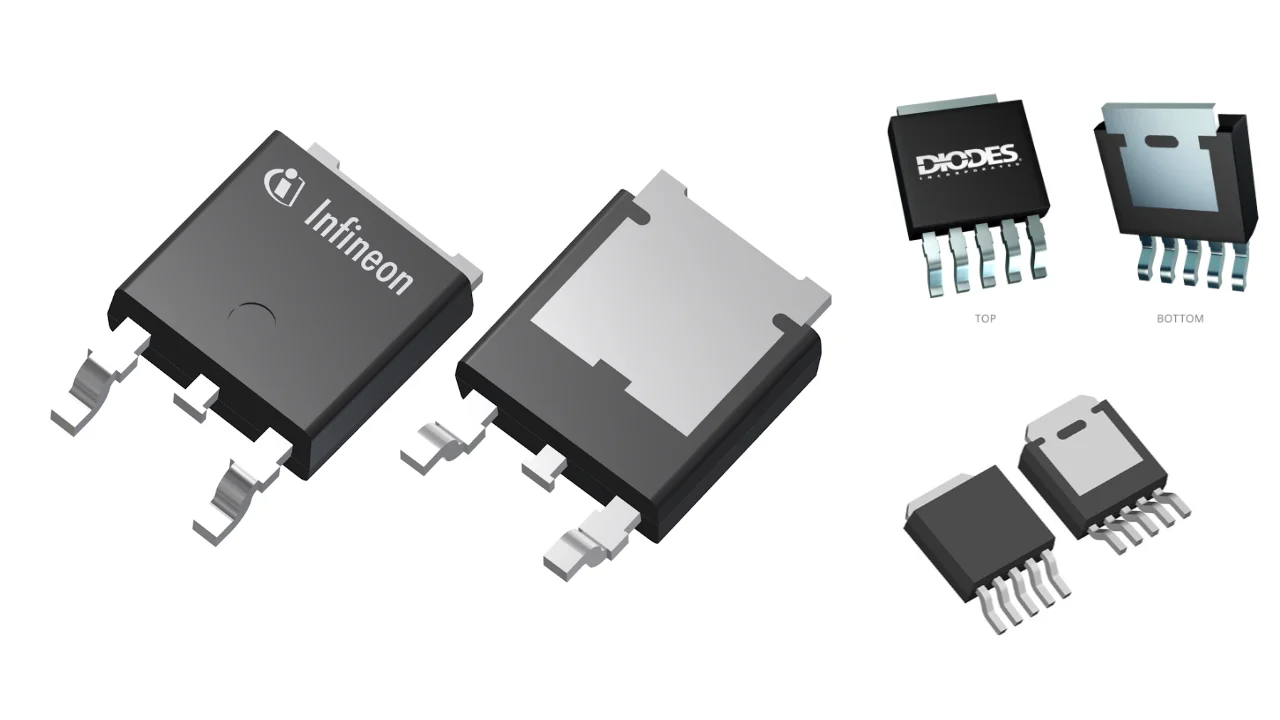
TO-252 (DPAK) Component Package The TO-252 component package family is a family of SMD component packages commonly used for MOSFETs and linear power regulators. It includes the 3-lead variant (DPAK) and 2 less commonly used 5-lead variants.
TO-252 (DPAK) Component Package The TO-252 component package family is a family of SMD component packages commonly used for MOSFETs and linear power regulators. It includes the 3-lead variant (DPAK) and 2 less commonly used 5-lead variants.
TO-253-4 Component Package TO-253-4 is a synonym (along with TO-253AA) for the SOT-143 component package.
TO-253-4 Component Package TO-253-4 is a synonym (along with TO-253AA) for the SOT-143 component package.
TO-253AA Component Package TO-253AA is a synonym (along with TO-253-4) for the SOT-143 component package.
TO-253AA Component Package TO-253AA is a synonym (along with TO-253-4) for the SOT-143 component package.
TO-261-4 Component Package TO-261-4 is a synonym for the SOT-223-3 (SOT-223 with 3 pins and 1 tab) component package.
TO-261-4 Component Package TO-261-4 is a synonym for the SOT-223-3 (SOT-223 with 3 pins and 1 tab) component package.
TO-261AA Component Package TO-261AA is a synonym for the SOT-233-3 (SOT-223 with 3 pins and 1 tab) package.
TO-261AA Component Package TO-261AA is a synonym for the SOT-233-3 (SOT-223 with 3 pins and 1 tab) package.
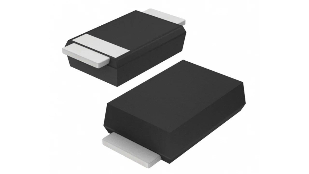
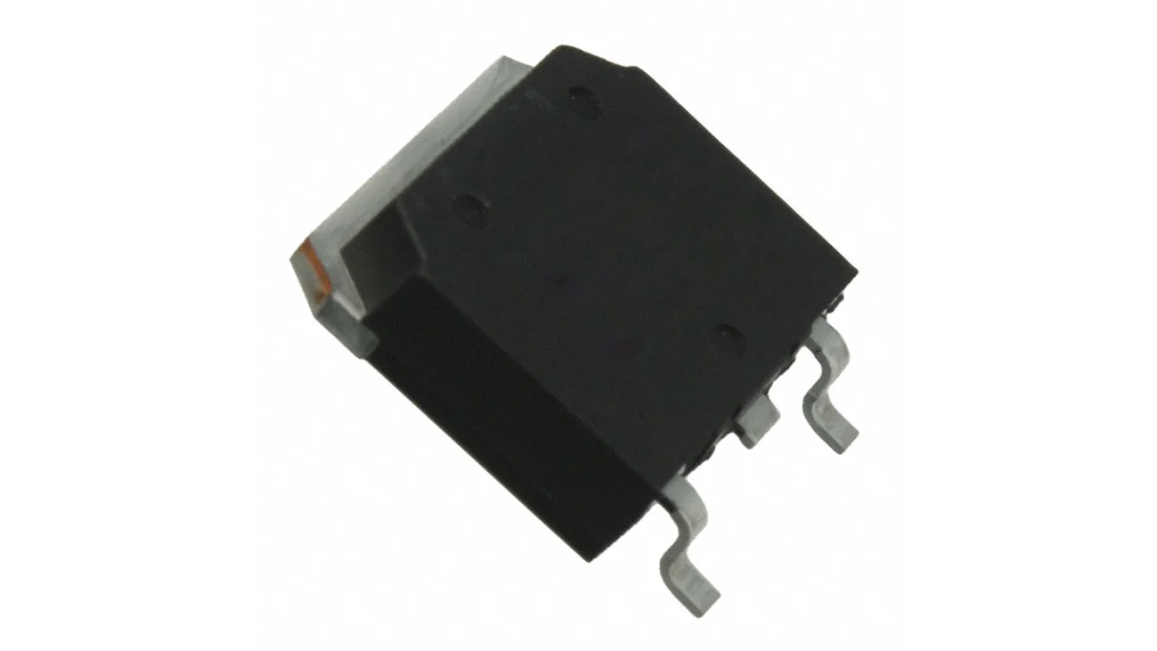
TO-263 (D2PAK) is a large SMD component package commonly used for high power MOSFETs, LDOs and SMPS.
TO-263 Component Package TO-263 (D2PAK) is a large SMD component package commonly used for high power MOSFETs, LDOs and SMPS.
TO-268 (D3PAK) Component Package TO-268 (D3PAK) is a SMD component package commonly used for high power MOSFETs, LDOs and SMPS. It is the 3rd in the series including TO-252 (DPAK) and TO-263 (D2PAK).
TO-268 (D3PAK) Component Package TO-268 (D3PAK) is a SMD component package commonly used for high power MOSFETs, LDOs and SMPS. It is the 3rd in the series including TO-252 (DPAK) and TO-263 (D2PAK).
TO-273AA Component Package TO-273AA is is a through-hole component package which can be considered an upgrade of the TO-220 with a clip-mounted design.
TO-273AA Component Package TO-273AA is is a through-hole component package which can be considered an upgrade of the TO-220 with a clip-mounted design.
TO-277A (SMPC) Component Package TO-277A (SMPC) is a high-power SMD component package.
TO-277A (SMPC) Component Package TO-277A (SMPC) is a high-power SMD component package.
TO-279 is a synonym for the TO-263 THIN component package.
TO-279 Component Package TO-279 is a synonym for the TO-263 THIN component package.
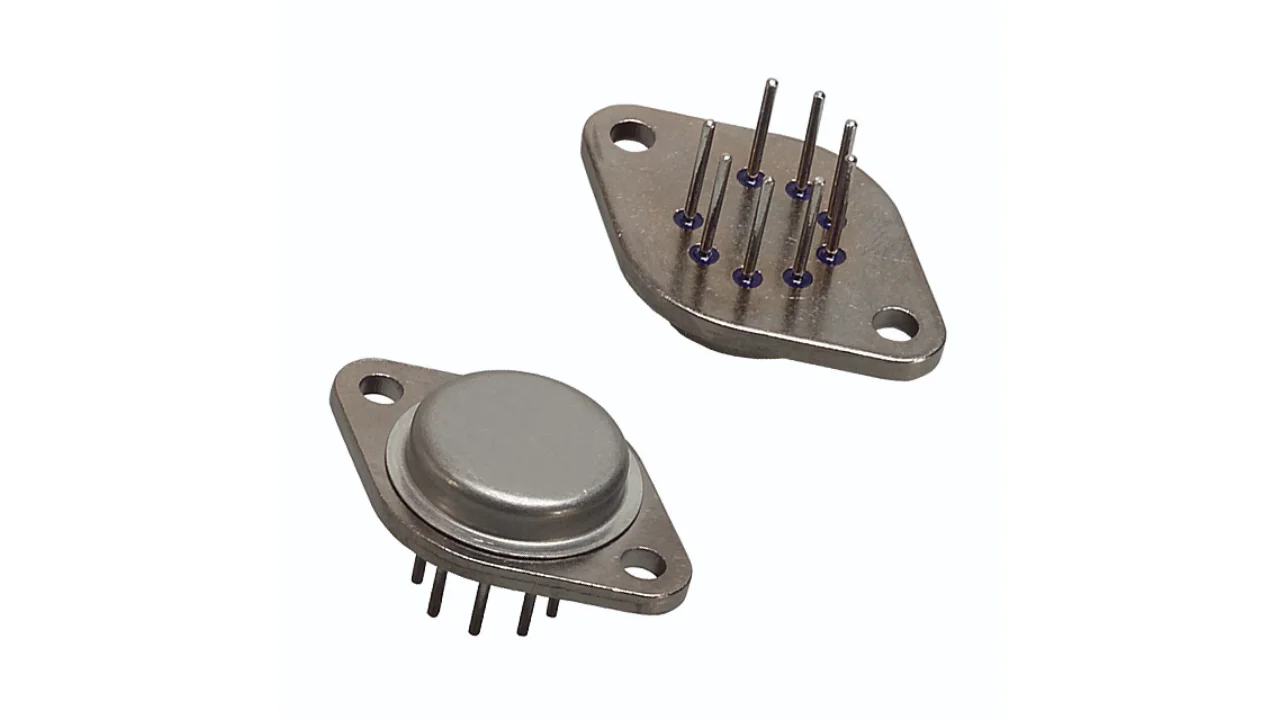
TO-3 is a family of large through-hole metal can packages used for things such as transistors, linear regulators and op-amps. There are 2 lead (common), 3 lead (common), 8 lead (rare), and 15 lead (very rare) variants.
TO-3 Component Package TO-3 is a family of large through-hole metal can packages used for things such as transistors, linear regulators and op-amps. There are 2 lead (common), 3 lead (common), 8 lead (rare), and 15 lead (very rare) variants.
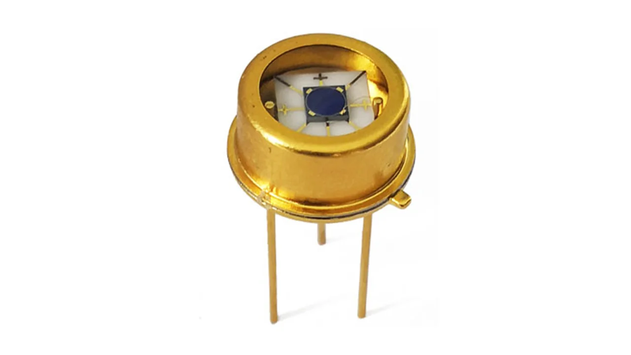
TO-39 is a family of metallic can packages used for hermetically sealing semiconductor devices.
TO-39 Component Package TO-39 is a family of metallic can packages used for hermetically sealing semiconductor devices.
TO-46 is a synonym for the TO-206AB component package.
TO-46 Component Package TO-46 is a synonym for the TO-206AB component package.
TO-5 is a family of through-hole can component packages. Variants exist with 3, 6, 8 and 10 pins.
TO-5 Component Package TO-5 is a family of through-hole can component packages. Variants exist with 3, 6, 8 and 10 pins.
TO-52 is a synonym for the TO-206AC component package.
TO-52 Component Package TO-52 is a synonym for the TO-206AC component package.
TO-72 is a synonym for the TO-206AF component package.
TO-72 Component Package TO-72 is a synonym for the TO-206AF component package.
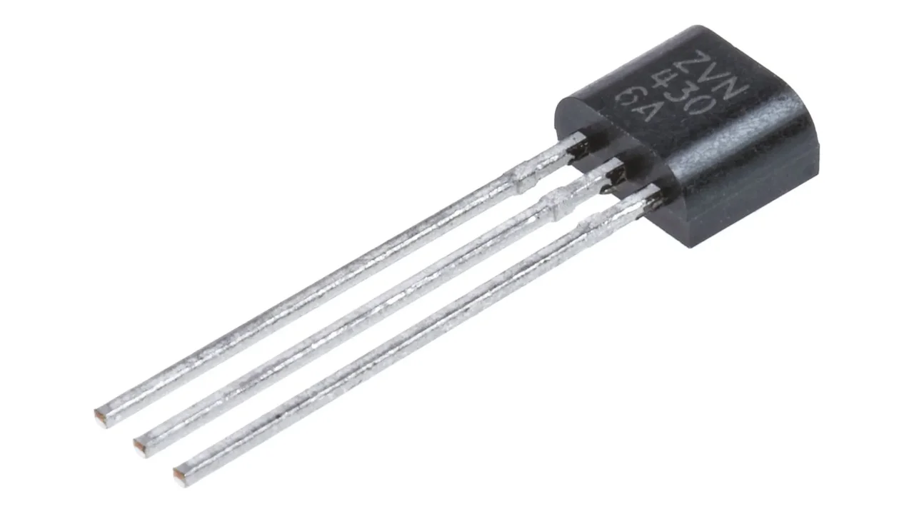
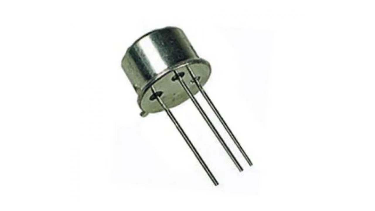
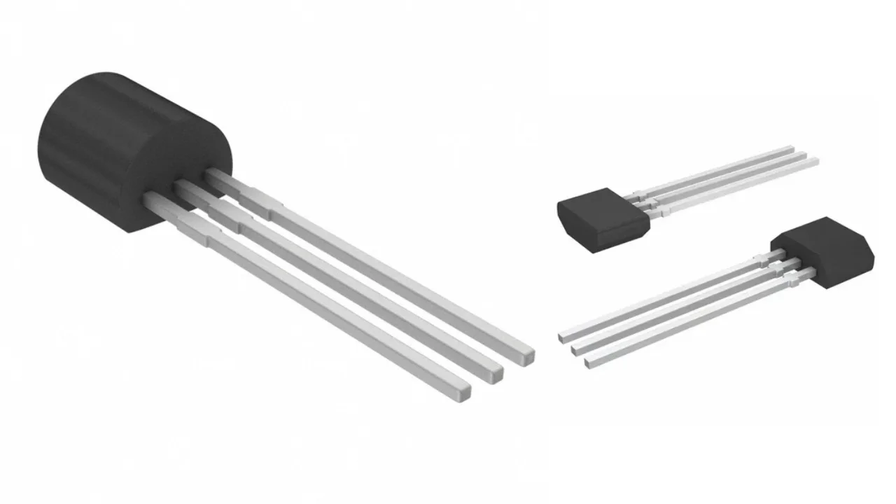
TO-92 (TO-226) Component Package TO-92 is a popular family of through-hole component packages for low-power through-hole transistors, MOSFETs, and linear regulators.
TO-92 (TO-226) Component Package TO-92 is a popular family of through-hole component packages for low-power through-hole transistors, MOSFETs, and linear regulators.
TO-93 (TO-209AB) Component Package Variants, pin counts, pitch and more info about the TO-93 component package.
TO-93 (TO-209AB) Component Package Variants, pin counts, pitch and more info about the TO-93 component package.
Variants, pin counts, pitch and more info about the TO-99 component package.
TO-99 Component Package Variants, pin counts, pitch and more info about the TO-99 component package.
TO-Leadless Component Package
TO-Leadless Component Package
TO-PMOD-7 Component Package
TO-PMOD-7 Component Package
Variants, pin counts, pitches, solderability, thermal resistances, dimensions, land patterns, 3D models and more info for the TQFP component package.
TQFP Component Package Variants, pin counts, pitches, solderability, thermal resistances, dimensions, land patterns, 3D models and more info for the TQFP component package.
Variants, pin counts, pitches, solderability, thermal resistances, dimensions, land patterns, 3D models and more info for the TSOC component package.
TSOC Component Package Variants, pin counts, pitches, solderability, thermal resistances, dimensions, land patterns, 3D models and more info for the TSOC component package.
Synonyms, variants, dimensions, 3D models, land patterns and more info on the uSiP component package.
uSiP Component Package Synonyms, variants, dimensions, 3D models, land patterns and more info on the uSiP component package.
Synonyms, variants, dimensions, 3D models, land patterns and more info on the USON component package.
USON Component Package Synonyms, variants, dimensions, 3D models, land patterns and more info on the USON component package.
Synonyms, variants, dimensions, 3D models, land patterns and more info on the WSON component package.
WSON Component Package Synonyms, variants, dimensions, 3D models, land patterns and more info on the WSON component package.
Component Size Reference Chart
The below image shows is a printable component package comparison chart. It shows a number of popular SMD (and a few through-hole) packages which are drawn to scale (when printed on A4 paper, it will print with a 1:1 scale). Hopefully this gives you a visual guide to the different sizes of various things you may be considering adding to your PCB.
It is also available as a printable PDF . If you print to A4 paper it will print with a 1:1 scale (make sure to deselect “fit to size”).
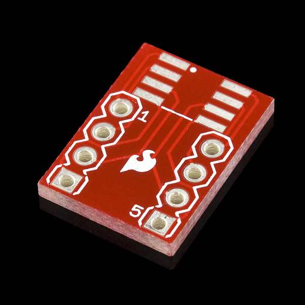
Break-out Boards
Break-out boards (a.k.a. IC adapters ) are useful for converting one package footprint into another. They are particular common for converting smaller SMT package footprints into 100mil DIP packages for prototyping with modern ICs.
If not brought from the right place, these break-out boards can be very expensive!
SparkFun is the cheapest supplier of break-out boards that I’ve found. Element14 also sells them, but at a much higher price.
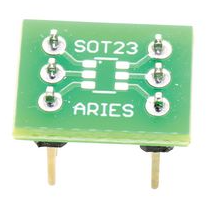
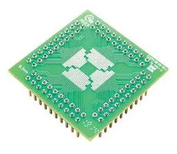
ARIES Correct-A-Chip Series
ARIES makes a nice range of not-to-expensive (for one-of prototyping use) breakout boards for a variety of SMD packages as part of their Correct-A-Chip product range. Three examples from this family are shown below.
Element14 stocks most of the range, which can be found at https://nz.element14.com/w/c/tools-production-supplies/prototyping-tools-breadboards/prototyping-ic-adapters?CMP=KNC-GOO-SHOPPING-2476033&product-range=correct-a-chip .
Leadframes
Leadframes are the metal structures that are use during the manufacturing of certain component packages (both through-hole and surface mount) to provide the electrical connection from the IC die to the outside world1
Examples of component packages that use leadframes:
Standards
The JEITA EIAJ ED-7500A standard (local copy ) has dimensions for TC-1 thru TB30, SC-1 thru SC-88A.
External References
If there is one other site I would direct you to for PCB information, it would be Tom Hausherr’s blog on the Mentor Graphics website.
3D models (which can be imported into Altium as step files) can be downloaded from 3D Content Central (www.3dcontentcentral.com ). It is a combination of content submitted from both users and suppliers, can contains many standard component packages in 3D.
SiliconFarEast “IC Package Types” (http://www.siliconfareast.com/ic-package-types.htm ) - A short but tidy graphical table describing most footprints. Also has data on the body size, body thickness, and lead pitch for the most common variants of each package.
The SMT Code Book (http://www.marsport.org.uk/smd/mainframe.htm ) - Handy database for working out what small SMT components are. Since there is usually not enough space to print the entire part number, most manufacturers print their own kind of code of small SMT components. This makes it really hard to determine what they are. To make matters worse, many manufacturers use the same code for different components, and sometimes the manufacturer releases two components with the same code! The trick is to be able to identify the package and the code, and together you can get a good idea of what the component is. The SMT Code Book lists over 3,500 SMT device codes in alphabetical order.
Answers.com’s Surface-mount Technology page . Broad spectrum of information regarding SMT components, the production methods and package sizes.
Suggested Pad Layouts For A Number Of Packages (Diodes INC) - Many recommended pad layouts/land patterns for common packages all in one PDF!
Quick-tecks SMT Package Dimensions PDF, which contains hundreds of dimensions for common SMD component packages. You can download it from here , or alternatively, use the local link [here](/docs/Quick-tecks SMT Package Dimensions.pdf).