BJT Common Collector Amplifier

The BJT common-collector amplifier is one of the three basic single-stage BJT amplifier topologies. The common collector amplifier topology is also known as a emitter follower amplifier or voltage follower. It has a high input-impedance, a low output-impedance, and has a non-inverting gain of around 1. It does NOT produce voltage gain, but is able to provide current gain, and therefore overall power gain. Because of it’s “buffering” capabilities it is often used between high-impedance inputs and low-impedance outputs (i.e. it is good for driving power-hungry loads)1.
The MOSFET analogue to the BJT common collector amplifier is the common drain amplifier.
This is a placeholder for the reference: tbl-bjt-common-collector-amplifier-properties shows the basic properties of the common collector amplifier, along with relative ratings for each compared to other amplifiers.
| Property | Value |
|---|---|
| Voltage Gain | Low |
| Current Gain | High |
| Power Gain | Medium |
| Input Impedance | High |
| Output Impedance | Low |
| Phase Shift | 0° |
Basic Common Collector Amplifier
A schematic of a basic common-collector BJT amplifier is shown in This is a placeholder for the reference: fig-common-collector-bjt-amplifier-basic-schematic.
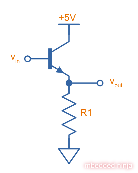
The output voltage is almost equal to the input voltage, except for an approximately diode drop across the base-emitter junction. This means that the amplifier has a voltage gain of almost unity (1), or .
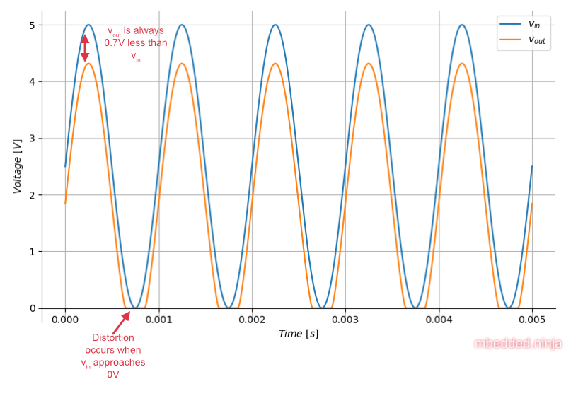
This is a placeholder for the reference: fig-basic-common-collector-amplifier-plot-annotated shows a graph of vs. for the circuit in This is a placeholder for the reference: fig-common-collector-bjt-amplifier-basic-schematic, with .
The common-collector amplifier is simulated in circuitjs below:
Common Collector Amplifier With AC Coupling And DC Bias
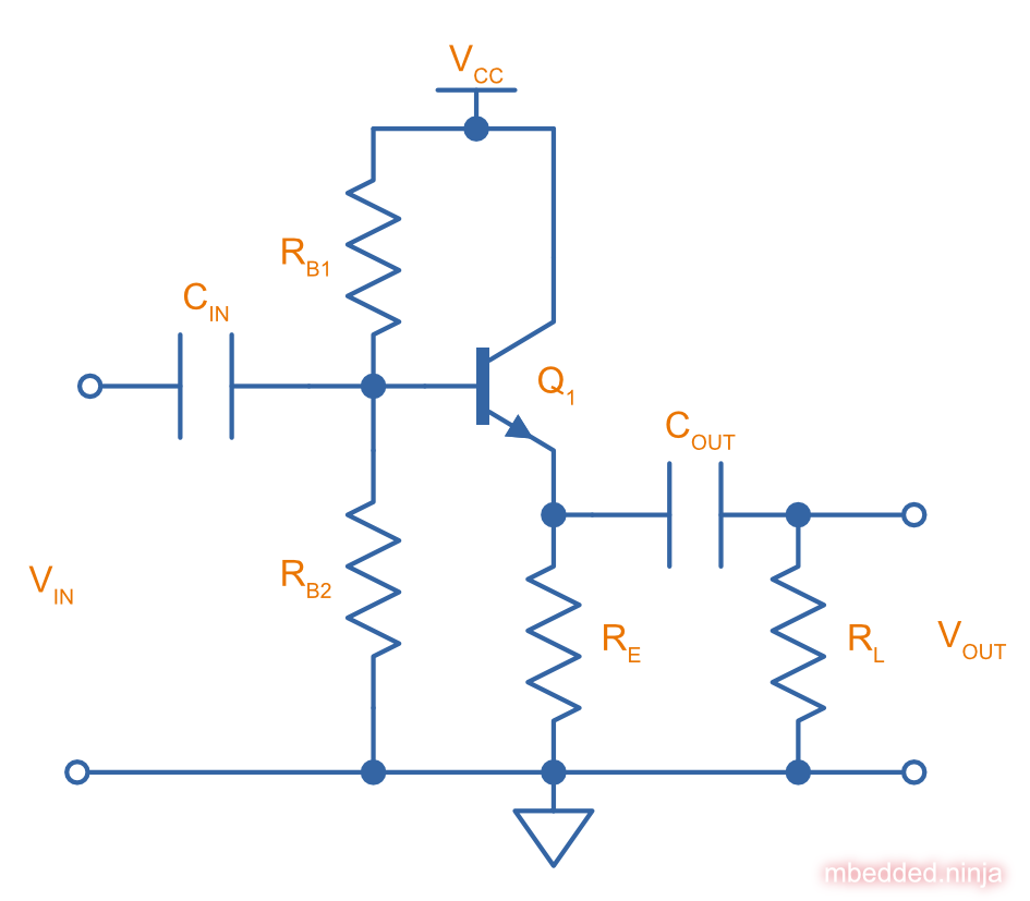
A more useful common-collector amplifier can be made which AC couples the input and provides a DC bias point at the base of the BJT. A schematic of one built with a NPN transistor is shown in This is a placeholder for the reference: fig-common-collector-bjt-amplifier-ac-coupled-schematic.
The small-signal AC model for this circuit is shown in This is a placeholder for the reference: fig-common-collector-bjt-amplifier-ac-coupled-ac-equivalent-schematic. DC voltage rails and capacitors are shorted.
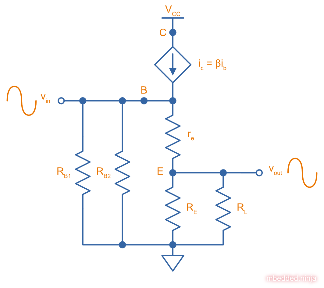
is the small-signal emitter resistance which is internal to the BJT.
Unloaded Voltage Gain
The unloaded small-signal voltage gain of a common-collector amplifier is found by ignoring in the small-signal AC model of the common-collector circuit. By definition the gain is:
Remember that and are lower case and represent changes in the signal (i.e. deltas, and ignore their DC levels). So a change in is just a change of emitter voltage, and a change in is just a change in base voltage. We can also apply Ohm’s law to get:
Input Impedance
The input impedance looking into the base of the transistor is:
Then the total input impedance is the base input impedance in parallel with both base resistors:
Further Reading
Common-Collector Amplifier Design by Kenneth A. Kuhn goes into great detail about the amplifier design with precise equations and considerations2. It’s much better than what I have here!
Footnotes
-
James M. Fiore (2022, May 23). Common Collector Amplifier. LibreTexts: Engineering. Retrieved 2022-08-11, from https://eng.libretexts.org/Bookshelves/Electrical_Engineering/Electronics/Book%3A_Semiconductor_Devices_-_Theory_and_Application_(Fiore)/07%3A_BJT_Small_Signal_Amplifiers/7.4%3A_Common_Collector_Amplifier. ↩
-
Kenneth A. Kuhn. Common-Collector Amplifier Design. Retrieved 2022-09-03, from https://www.kennethkuhn.com/students/ee351/bjt_cc_amplifier_design.pdf. ↩ ↩2