Microstrips

Microstrips are impedance controlled transmission lines on the top or bottom layers of a PCB, where there is free space above the track, and a copper pour on the layer below the track. This is opposed to striplines, which are embedded in a middle layer of a PCB, and have a copper pour above and below them.
RFcafe Equations
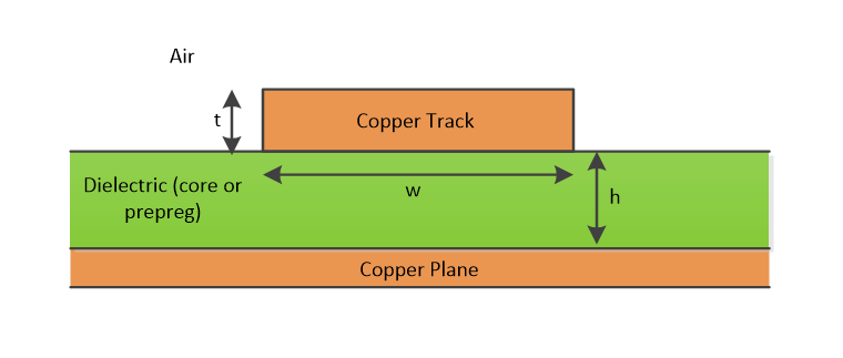
To calculate the impedance of a microstrip, we need to know the following parameters of the PCB:
= width of the track (in meters)
= thickness of the track (in meters)
= thickness (or height) of the substrate (in meters)
= the dielectric constant of the PCB substrate
The following equations can then be used to calculate the impedance of the microstrip. First we calculate the intermediary values and .
Then we can calculate the effective dielectric, and then the track impedance, . There are different equations to be used depending on the ratio of to :
If :
If :
\begin{align} \epsilon_{eff} = \frac{\epsilon_r + 1}{2} + \frac{\epsilon_r - 1}{2\sqrt{1 + 12\frac{H}{W}}} $$ </div> \end{align}Equations are from http://www.rfcafe.com/references/electrical/microstrip-eq.htm.
Microstrip Impedance Calculator
Use the calculator below to apply these equations directly. Enter the track width, copper thickness, substrate height and substrate dielectric constant, picking the units for each dimension from the dropdowns.
The Equations Altium Uses
The equation Altium uses (as of AD14, and in unsimplified form):
where:
= track width
= track to plane height
= track height (thickness)
= desired characteristic impedance
= dielectric of material between track and plane
Or in computer equation form:
w = ((5.98*h1)/exp(Z/(60/sqrt(Er*(1-exp(-1.55*(0.00002+h1)/h1)))))-h2)/0.8Modes Of Propagation
The primary and desired mode of signal propagation in a microstrip is transverse electric and magnetic (TEM). Other modes are undesirable and increase the degradation of the signal, such as what occurs with microstrip dispersion (see below).
Microstrip Dispersion
With wide microstrips that are far away from the ground plane, strange modes of propagation appear. Significant energy can now bounce between the microstrip and ground plane. Parts of the waveform that bounce between the microstrip and ground plane take longer to travel down the microstrip, distorting the waveform. This is called microstrip dispersion. Microstrip dispersion compounds quadratically with trace-to-ground height.
Why not then make the ground plane really close to the microstrip then? Well, the skin-effect resistance varies inversely proportional with trace width (remember that for a given impedance, if the height between microstrip and ground is decreased, the trace width also has to decrease). So there is a trade-off point where both effects are minimised to an agreeable level.
Design Guidelines
A rule of thumb is to keep co-planar ground at least 3x the microstrip width away from the edges of the microstrip. Close, co-planar ground reduces the impedance of the microstrip. In fact, putting the ground too close to the microstrip results in you making a co-planar waveguide (CPW) instead!