Digital Logic

Published On:
Aug 6, 2012
Last Updated:
Apr 4, 2023
Digital logic is the study and application of the fundamentals in digital (binary) electronics, e.g. gates, flip-flops, state machines.
See the Gates page for info on how NOT, AND, OR, NOR, and NAND gates work, what they are used for,
See the Latches and Flip-Flops page for more information on how circuit “memory” can be made and how level-triggered latches and edge-triggered flip-flops work.
Child Pages
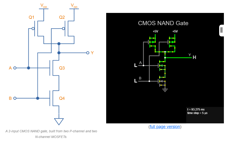
An overview of the different types of digital logic gates, including NOT, AND, NAND, OR, NOR, XOR, XNOR, and how they are constructed from diodes, transistors, and MOSFETs.
Gates
An overview of the different types of digital logic gates, including NOT, AND, NAND, OR, NOR, XOR, XNOR, and how they are constructed from diodes, transistors, and MOSFETs.
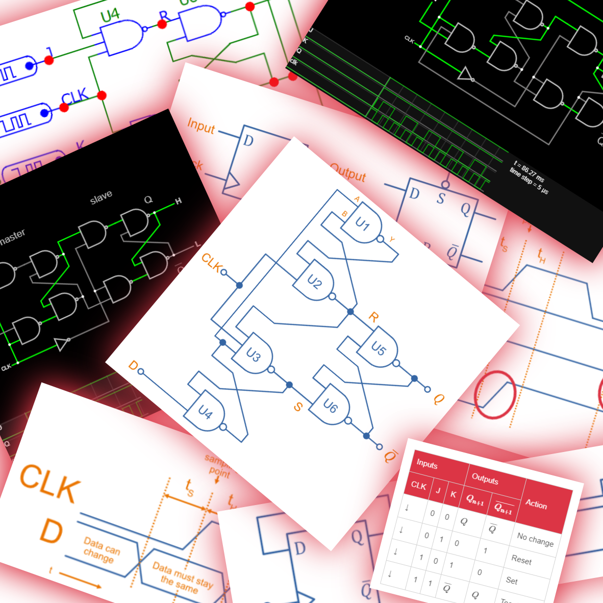
SR, D and JK latches and flip-flops, how they work, schematics, simulations, timing requirements and more.
Latches and Flip-Flops
SR, D and JK latches and flip-flops, how they work, schematics, simulations, timing requirements and more.