BJT Common Emitter Amplifier

The BJT common emitter amplifier is a general-purpose BJT-based amplifier that is typically used for voltage amplification. It offers great voltage gain and ok current gain. The input impedance is moderate but unfortunately it has high output impedance. The output is inverted with respect to the input. It is commonly followed with a buffer circuit such as a common-collector amplifier to reduce the output impedance. The common emitter amplifier finds use in audio and RF applications.
The MOSFET analogue to the BJT common emitter amplifier is the common source amplifier.
The table below shows the basic properties of the common emitter amplifier, along with relative ratings for each compared to other amplifiers.
| Property | Value |
|---|---|
| Voltage Gain | High |
| Current Gain | Medium |
| Power Gain | Medium |
| Input Impedance | Medium |
| Output Impedance | High |
| Phase Shift | 180° |
How A Common Emitter Amplifier Works
The schematic below shows a common emitter amplifier with DC bias and AC coupling.
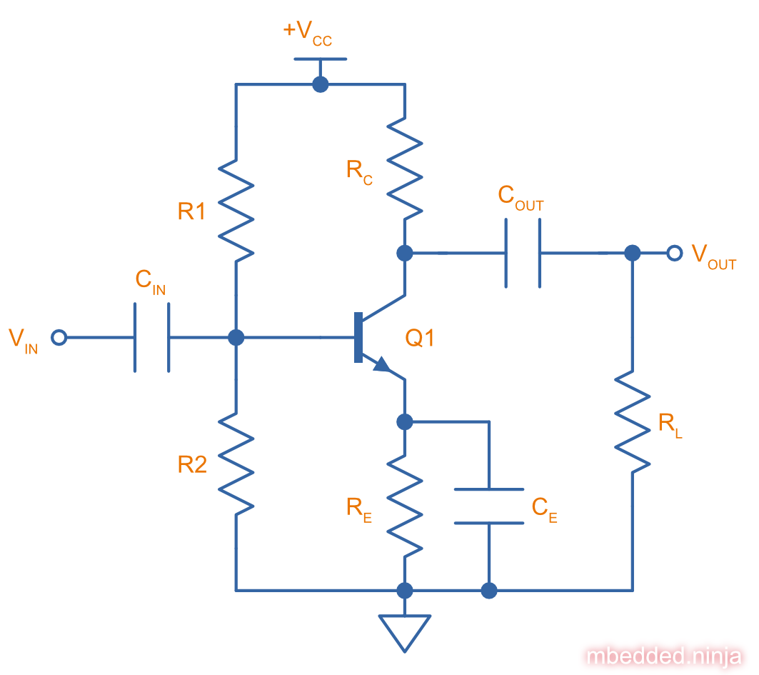
- and are used to provide a DC bias point for the base of the transistor, using the standard resistor divider technique (to be exact, you also have to take into account that the transistor draws some current from the output of the resistor divider, but generally you can ignore that).
- is used to AC couple the input signal to the DC bias point — its value is chosen so that it appears as a short for the AC signal frequencies of interest but blocks DC.
- adds emitter degeneration1 and makes the amplifier gain more stable with variations in . is the emitter bypass capacitor and is used to bypass so that the AC signal essentially sees the emitter connected directly to ground.
- is the collector resistor which helps set the voltage gain of the amplifier. Sometimes this is called the load resistor2, however this can be confusing, as typically the “load” is placed after the output AC coupling capacitor.
- is the load resistance. You may see this and omitted from some diagrams of the common emitter amplifier.
- is the AC coupling capacitor on the output, which blocks the DC component, similarly to .
Gain Of A Common Emitter Amplifier
The diagram below is used to derive the gain equation for a common emitter amplifier.
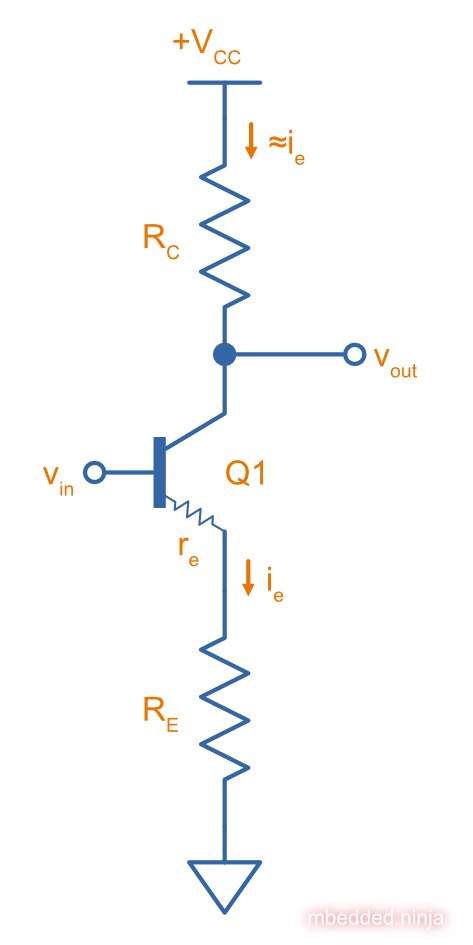
The voltage gain of a common-emitter amplifier (by definition) is:
Remember that and are lower case and represent changes in the signal (i.e. deltas, and ignore their DC levels). Now, assuming , the change in voltage at the output is:
And the change in voltage at the input is:
Note that we have to take the internal emitter resistance into account here, as the emitter bypass capacitor is going to remove the term further down, leaving only .
Substituting these equations for and into the gain equation gives:
Remember that the value for is dependent on the emitter current at the DC bias point:
Thus, for our signal frequencies at which the capacitor shorts out external resistor , the emitter resistance is just and the gain becomes:
Common Emitter Amplifier Design Process
How do you design a common emitter amplifier? Let’s do a worked example to progress through the design steps.
Assumptions
- is
- We’ll be using the venerable BC548B NPN transistor from onsemi in our amplifier.
- We’re trying to get as much gain as possible (a noble quest).
Steps
-
Choose collector current: Choose a suitable DC collector current for your amplifier. A reasonable choice would be (max. for the BC548B is ).
-
Determine the emitter resistor : As a rule of thumb, 10% of is normally dropped across 3 4:
And then:
-
Find the collector resistor : We are dropping across the emitter resistor. That leaves to be dropped across the collector resistor and the BJT. Assuming a saturation voltage of , this gives the BJT of swing. For maximum symmetrical output, we want to drop half of this across the collector resistor:
-
Find the base current: Calculate using the approximate gain:
-
Determine the base voltage : is just the emitter voltage plus the diode drop:
-
Calculate resistor divider values: Choose and to set the output of the resistor divider to match this base voltage. We also want to make sure the current flowing through the resistor is 10x the current that will be sucked out of it into the base of the transistor, that way we can ignore the loading of the BJT when calculating the resistor values.
Now we can easily calculate the value of :
And :
-
Calculate input AC coupling capacitor: The rule of thumb is to make sure the impedance of the capacitor is 10x less than the AC impedance of the resistor divider at the lowest frequency of interest5. Our lowest frequency of interest is .
-
Calculate emitter bypass capacitor: The same rule of thumb applies to , except this time its impedance should be 10x smaller than :
-
Calculate the gain:
Or in dB:
-
Done!
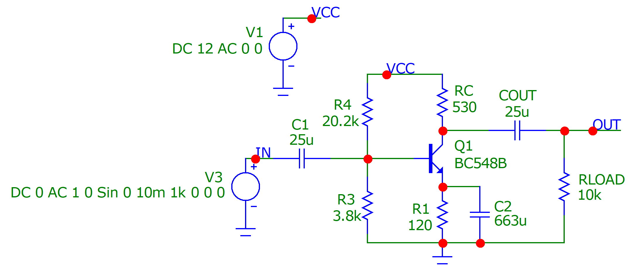
The finished schematic, along with voltage sources ready for simulation is shown below.
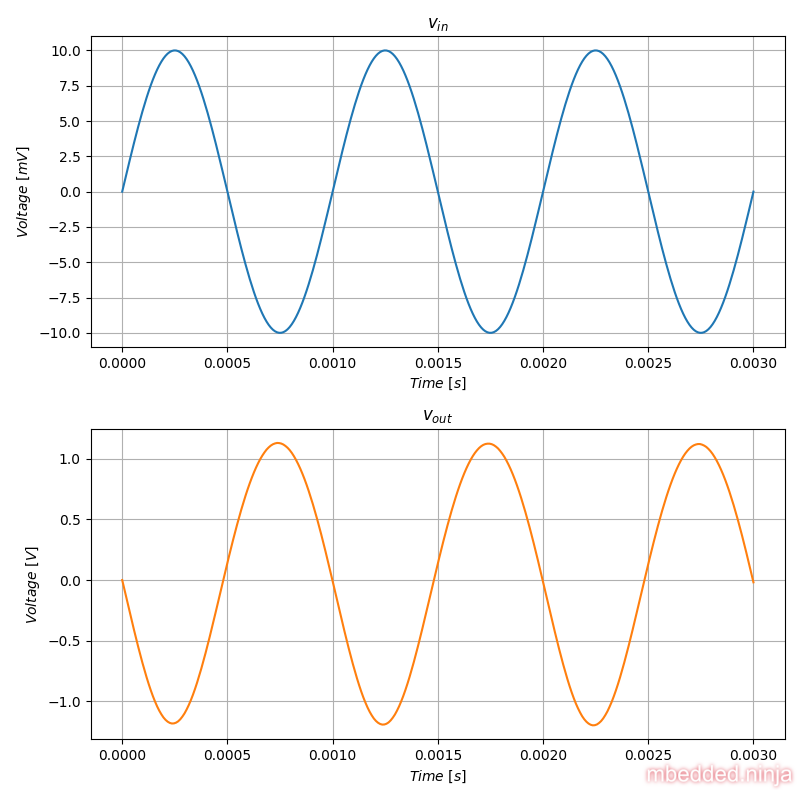
Given the large gain of , I didn’t want to saturate the output so I chose an input sine wave signal with an amplitude of at a frequency of . The simulated input and output voltages are shown below (note the change in the y-axis scale - the input is in and the output is in ).
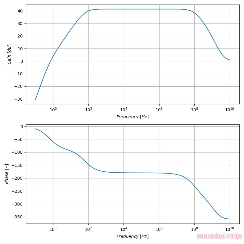
The simulated frequency response shown below is close to what we expect. The simulated gain of around is close enough to our calculated gain of considering all the approximations we made! Part of the difference is due to loading the output (with the load connected the gain is ), with the rest due to the simulated bias current (and hence ) not exactly matching our design values. The phase shift is for most of our signal bandwidth.
Footnotes
-
Analog Devices (2020, Mar 23). Activity: Common Emitter Amplifier [wiki]. Retrieved 2022-08-20, from https://wiki.analog.com/university/courses/electronics/electronics-lab-5. ↩
-
Bob Harper (2018, Dec). Common Emitter Transistor Amplifier [article]. Diyode. Retrieved 2022-08-21, from https://diyodemag.com/education/common_emitter_transistor_amplifier. ↩
-
Stack Exchange: Electrical Engineering (2021, Oct 13). How to choose resistors’ value for common emitter amplifier? [forum post]. Retrieved 2022-08-17, from https://electronics.stackexchange.com/questions/127491/how-to-choose-resistors-value-for-common-emitter-amplifier. ↩
-
Electronics Notes. Transistor Common Emitter Circuit Design [article]. Retrieved 2022-08-20, from https://www.electronics-notes.com/articles/analogue_circuits/transistor/transistor-common-emitter-amplifier-circuit-design.php. ↩
-
Electronics Tutorials. Common Emitter Amplifier [article]. Retrieved 2022-08-18, from https://www.electronics-tutorials.ws/amplifier/amp_2.html. ↩