Gates

Logic gate inputs are normally labelled as a single letter, starting with A (e.g. a three input AND gate would have inputs A, B and C). The output is normally labelled Y (in other material you may see this labelled X), unless you are using a flip-flop or latch, and the output is labelled Q.
There are a few different standards used to draw logic gates on schematics:
- MIL-STD-806B (Graphic Symbols For Logic Diagrams): The most commonly used symbols for basic and/or/xor etc. gates are captured in this standard. Each gate has a unique shape and is easily distinguished on a large schematic with many gates. NOT logic is shown with a bubble.
- IEC 60617 (ANSI/IEEE Std 91-1984): All the gates are IC-like rectangles with symbols inside to denote the function. NOT logic is shown with a flag on the pin rather than a bubble. Not as easy to quickly identify the gate as MIL-STD-806B, and not as widely used.
- DIN 40700-24 (Graphical Symbols; Components For Precision Engineering Devices, Especially Clocks): Even rarer than the MIL-STD-806B or IEC 60617 symbols, these are rarely seen. The 1976 Edition was released in June 1976. DIN symbols on this page are referenced to https://de.wikipedia.org/wiki/Logikgatter#Typen_von_Logikgattern_und_Symbolik.
This page uses the convention of TRUE or 1 to represent the logic state true, and FALSE or 0 to represent the logic state false.
Types of Gates
NOT
Arguably the simplest logical gate (ignoring a buffer), a NOT gate (a.k.a. inverter) always outputs the opposite (complement) of the input. If the input is TRUE, the output is FALSE. If the input is FALSE, the output is TRUE.

The truth table for a NOT gate is:
| Inputs | Output |
|---|---|
| A | Y |
| 0 | 1 |
| 1 | 0 |
And this gives rise to the simple equation for NOT logic:
AND
An AND gate outputs TRUE only if all its inputs are TRUE. AND is also called logical conjunction1.

Truth table for an AND gate is:
| Inputs | Output | |
|---|---|---|
| A | B | Y |
| 0 | 0 | 0 |
| 0 | 1 | 0 |
| 1 | 0 | 0 |
| 1 | 1 | 1 |
The equation for the AND logic may be written in one of the following ways:
An AND gate can be made using basic diode logic as shown below:

NAND
A NAND gate is just an AND gate but with the output inverted. This is shown below with the bubble at the output of the AND symbol:

Truth table for a NAND gate:
| Inputs | Output | |
|---|---|---|
| A | B | Y |
| 0 | 0 | 1 |
| 0 | 1 | 1 |
| 1 | 0 | 1 |
| 1 | 1 | 0 |
OR
An OR gate is TRUE if at least one input is TRUE. This means it also outputs TRUE if all its inputs are TRUE. OR is also called logical disjunction1.

Truth table for an OR gate:
| Inputs | Output | |
|---|---|---|
| A | B | Y |
| 0 | 0 | 0 |
| 0 | 1 | 1 |
| 1 | 0 | 1 |
| 1 | 1 | 1 |
The OR operation can be expressed in an equation in the following ways:
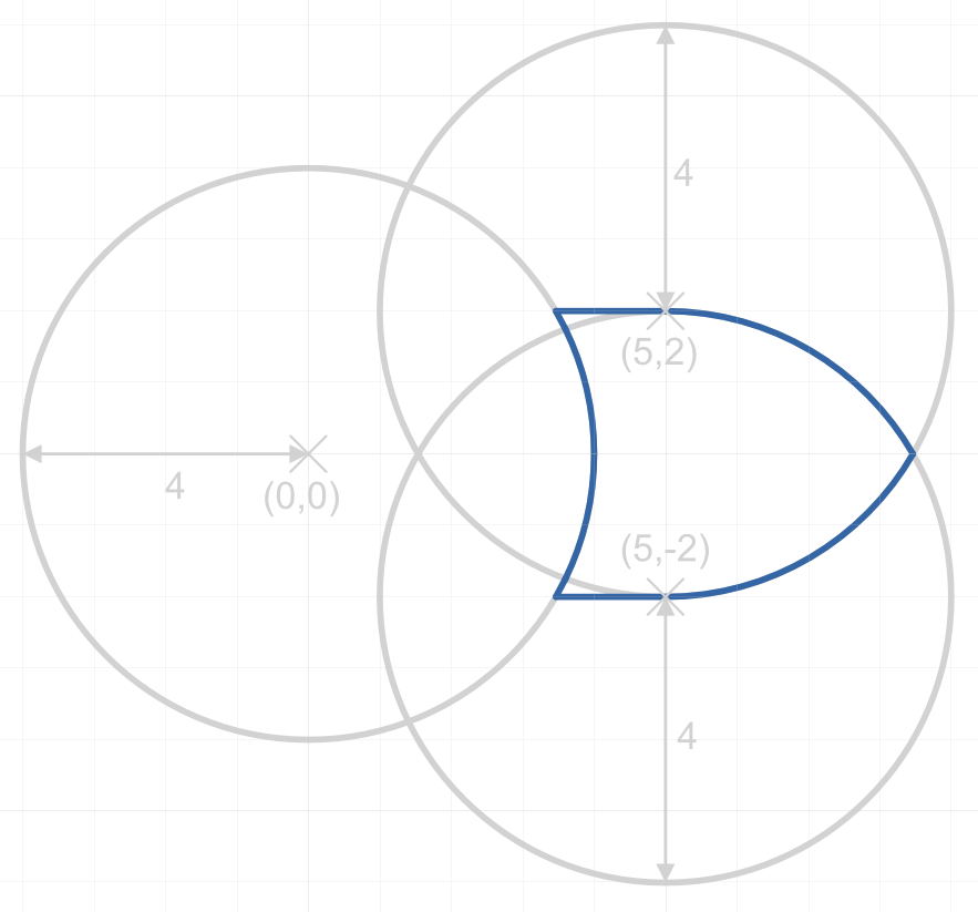
The OR gate be drawn using three equal diameter circles placed on a grid as shown in the below image. Segments of the circles perimeters are taken along with the addition of two horizontal line sections to form the classic OR gate shape2.
NOR
A NOR gate is just an OR gate but with the output inverted (i.e. what you would get if you connected the output of an OR gate to an inverter). Just like the NAND gate, the NOR gate is shown in the below image — and is just an OR gate symbol with a bubble on the output.

Truth table for a NOR gate:
| Inputs | Output | |
|---|---|---|
| A | B | Y |
| 0 | 0 | 1 |
| 0 | 1 | 0 |
| 1 | 0 | 0 |
| 1 | 1 | 0 |
The equation for a NOR gate:
XOR
A 2-input XOR gate (exclusive OR) only outputs TRUE if one and only one of its inputs is TRUE. For many gate construction technologies, the XOR gate is the most complex primitive gate to build.

Truth table for a 2-input XOR gate:
| Inputs | Output | |
|---|---|---|
| A | B | Y |
| 0 | 0 | 0 |
| 0 | 1 | 1 |
| 1 | 0 | 1 |
| 1 | 1 | 0 |
The symbol is used to represent XOR, and hence XOR can be written in the following ways:
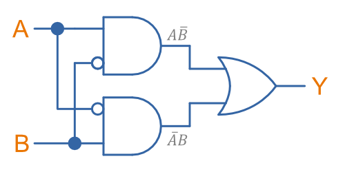
There are many ways to build XOR gates from the more basic NAND, NOR, AND and OR gates. The most intuitive approach to me is to represent the XOR gate as . The following circuit shows this structure:
The following circuit shows a XOR gate made from a AND, NAND and OR gate. This circuit implements the equation . Toggle the inputs in the right-hand side interactive simulation to see the XOR gate in action!

The below image shows a XOR gate made exclusively from NAND gates:

You can also make a XOR gate exclusively from NOR gates, as shown in the below image. Note that the structure is similar to the all-NAND gate version of the XOR, but with the additional inverting gate on the output.

Whilst it is intuitive how an AND or OR gate should work with more than 2 inputs, the same cannot be said for a XOR gate. Should the output be TRUE only if exactly one input is TRUE? Should the output be TRUE if at least 1 but not all of the inputs are TRUE? Or should the output be TRUE if one input is TRUE, FALSE for 2 inputs TRUE, TRUE again for 3 inputs TRUE, etc.? So in general, a XOR gate with more than 2 inputs is ill-defined. However, there are a few other names used for logic that performs some of these functions:
- Output TRUE only if 1 and only 1 input is TRUE. This is called a one-hot detector. However, this is rarely seen in practise.
- Output TRUE only if an odd number of inputs are TRUE. This is called a parity generator or modulo-2 adder.
XOR gates are used for:
- Parity generators: A sequence of XOR gates can calculate the parity of a block of data, which is used for simple single-bit error detection in some communication protocols (e.g. optional setting you can enable with UART)3.
- Correlation/sequence detection: XOR gates output
FALSEif both inputs are the same. This behaviour can be utilized to perform correlation between two bit streams. - Cryptographic circuits.
XNOR
The XNOR gate is an XOR gate but with the output inverted. The symbol is:

The truth table for an XNOR gate is:
| Inputs | Output | |
|---|---|---|
| A | B | Y |
| 0 | 0 | 1 |
| 0 | 1 | 0 |
| 1 | 0 | 0 |
| 1 | 1 | 1 |
Logic Families
Diode Logic (DL)
Diode logic (DL) is digital logic circuitry made from just diodes and resistors. It is a very simple (if not the simplest) way of constructing logic gates in a circuit. Diode logic is great for getting a basic theoretical understanding of how logic gates are realized, but is rarely used in practise due to fan-out, switching speed issues, and limited gate constructibility (more on this below)! Also known as diode-resistor logic (DRL).
Before long you’ll be struck with the solemn realization you can’t create a NOT gate (inverter) from pure diode logic (or any gates that require inverting capabilities, such as NAND or NOR gates). This limits you to being only able to make AND or OR gates, and hence its usefulness is severely limited. NOT gates are constructable as soon as you add switching elements, such as transistors. Resistor-transistor logic is the extension of diode logic but the addition of transistors.
Resistor-Transistor Logic (RTL)
Resistor-transistor logic (RTL) is one of the most basic families of digital logic (only diode logic beats it in terms of simplicity). It uses resistors and BJTs to build the basic gates required for digital logic. Nowadays it is completely superseded by logic families such as transistor-transistor logic (TTL) and CMOS. However, it serves as a great place to introduce readers on how logic gates are built from discrete components.

Advantages:
- Very basic to create.
- Uses a minimal number of transistors (this was important in the early days of IC fabrication as transistors were expensive!)
Disadvantages:
- Very limited fan-out.
- Significant power consumption: When the transistors are switched on.
- Weak drive in one direction: Single transistor strongly drives output only in one direction, pull-up/down resistor is used in opposite direction.
- Poor noise margins.

LOW, neither transistor is on and the output is pulled HIGH by . Any HIGH input will turn on a transistor, which will drive the output LOW.The Apollo Guidance Computer (AGC) used RTL logic. The AGC controlled and navigated the Apollo spacecraft to the Moon and back4.
Diode-Transistor Logic (DTL)
TODO: Add info here.
Transistor-Transistor Logic (TTL)
The inputs of TTL logic are the emitters of BJTs.
TTL NAND Gate
TTL NAND gates can use special multiple-emitter BJTs to reduce the transistor count. Each input of the NAND gate is connected to one of the emitters. In the case of a NPN BJT, if any 1 or more of the base-emitter junctions is forward biased, then the transistor turns on5.
N-type Metal-oxide Semiconductor Logic (NMOS)
N-type Metal-oxide Semiconductor (NMOS) logic is a way of building logic functions from N-channel MOSFETs. In the early days of digital logic (1970s), it was much faster and easier to manufacture than CMOS, however since the 1980s CMOS took over and has become the dominant way of implementing logic gates6. NMOS is built from an arrangement of N-channel MOSFETs on the low-side (depending on the function) and a pull-up resistor on the high side.
NMOS Inverter Gate
A NMOS inverter is simply made from a N-channel MOSFET and a resistor, as shown below:
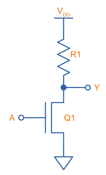
When the input is LOW, the N-channel MOSFET is turned OFF, and so the output is pulled HIGH by . When is HIGH, the N-channel MOSFET gets turned on. Its equivalent drain-source resistance drops to a value much lower than , and so therefore the output is effectively driven LOW, completing the inverter functionality.
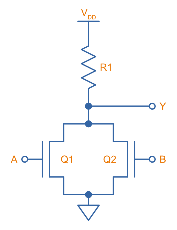
NMOS NOR Gate
The NMOS NOR gate uses two N-channel MOSFETs connected in parallel to drive the output LOW if either input is HIGH. If neither input is LOW, then no MOSFET will be on and the output will be pulled HIGH by the resistor.
Complementary Metal-oxide Semiconductor Logic (CMOS)
Complementary metal-oxide-semiconductor (CMOS) is a way of building logic functions from complementary pairs of N-channel and P-channel MOSFETs. Today, it is by far the most popular way of constructing digital integrated circuits (ICs)7. CMOS circuits typically have negligible static power dissipation and only consume power during transitions. It advances from NMOS technology by replacing the upper resistor with P-channel MOSFETs, which both eliminates static power dissipation and speeds up the low-to-high transition.
Represented by AC/ACT in part numbers, or HC/HCT for high-speed equivalents. The T in the logic subfamily name signifies the parts have TTL-compatible inputs.
CMOS Inverter Gate
The inverter is the easiest CMOS logic gate to make! It just consists of one P-channel and one N-channel MOSFET in a “totem-pole” configuration, as shown below. On the right-hand side is an interactive simulation.
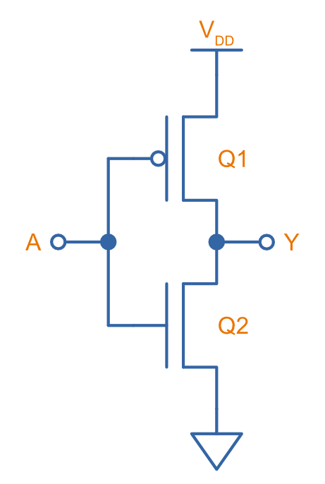
When the input is HIGH, the gate-source voltage of the bottom-side N-channel MOSFET is and turns the MOSFET ON. The top-side P-channel MOSFET’s gate-source voltage is and therefore OFF. Hence the output gets driven LOW. When is LOW, the bottom-side N-channel MOSFET’s gate-source voltage goes to and the P-channel’s gate-source voltage goes to , turning it ON and driving the output HIGH.
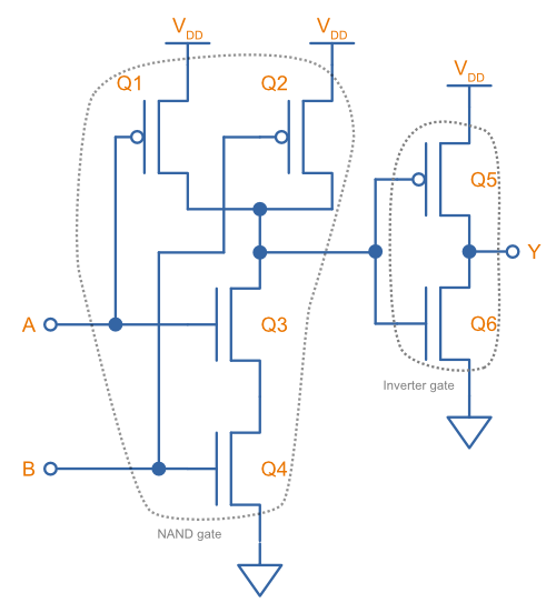
CMOS NAND Gate
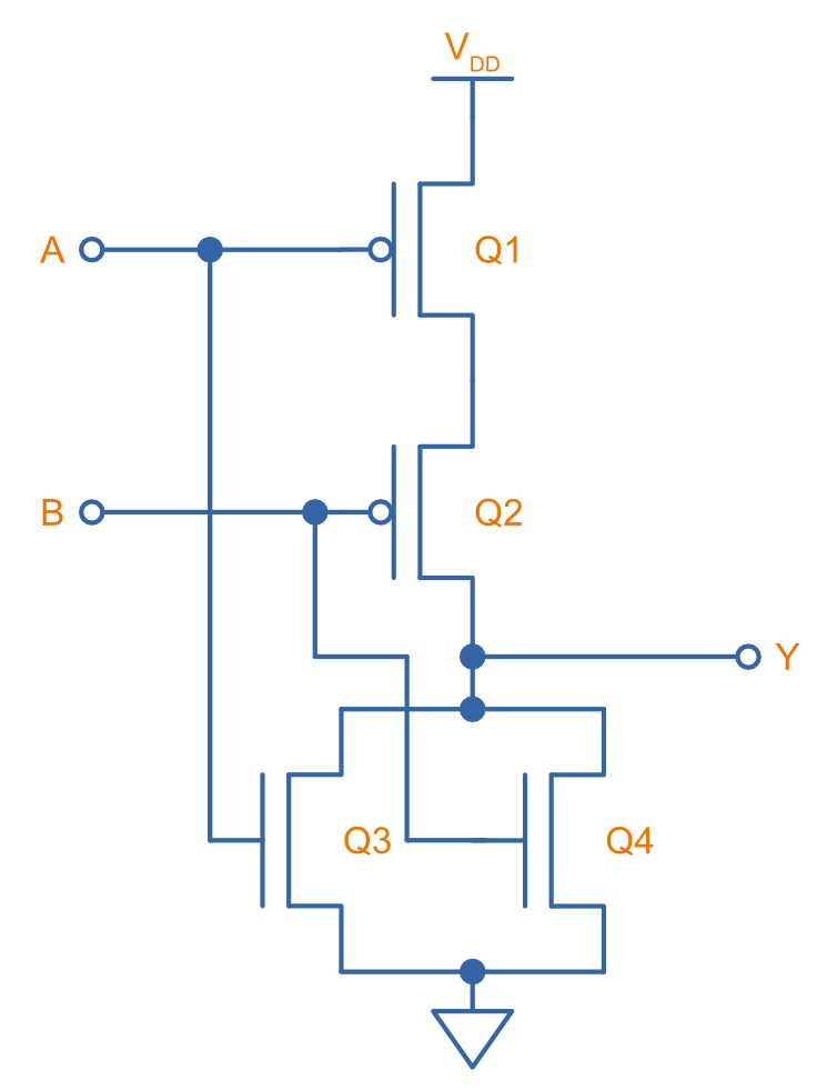
After the inverter, the two easiest CMOS gates to build are the NAND and NOR gates. A 2-input NAND gate can be built from two P-channel and two N-channel MOSFETs as shown below. On the right-hand is an interactive simulation.
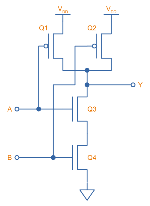
Two N-channels are connected in series on the bottom side, and two P-channels are connected in parallel on the top side. Both inputs ( and ) have to be HIGH to turn on both the lower side N-channel MOSFETs and drive the output () LOW. If either inputs are LOW, at least one of the high-side P-channel MOSFETs will be turned on, driving the output HIGH. This completes the NAND logic.
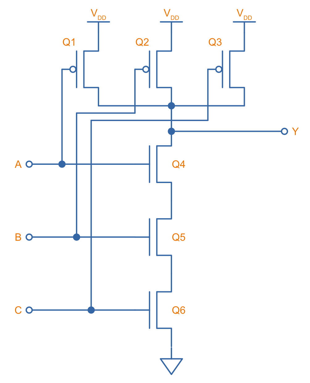
The number of inputs can be easily increased from 2 by adding the appropriate number of extra MOSFETs in series and in parallel. For example, a 3-input CMOS NAND gate’s schematic would look like this:
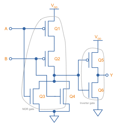
CMOS NOR Gate
A CMOS NOR gate is built in a similar fashion to a NAND gate, except you swap the serial and parallel connections of the P-channel and N-channel MOSFETs around. On the right-hand side is an interactive simulation.
CMOS AND Gate
Funnily enough, the easiest way to build a CMOS AND gate is to build a NAND gate and then add an inverter on its output. Thus its schematic looks like what is shown in the below-left picture.
CMOS OR Gate
In a similar fashion to the CMOS AND gate, the simplest way to build a CMOS OR gate is to build a NOR gate and then add an inverter on its output.
CMOS XOR Gate
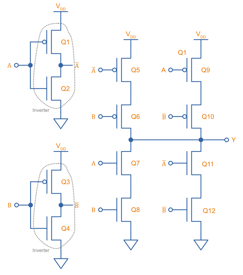
The CMOS XOR gate is the hardest CMOS gate primitive to build! It can be built with the circuit shown below, which uses a total of 12 MOSFETs, 3 times as many as the basic NAND and NOR gates!8
Have a play around with the interactive XOR gate simulation below:
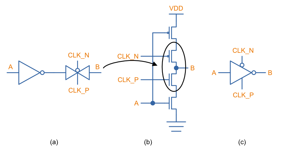
Tristate CMOS Inverter
A useful building block for digital logic is a CMOS inverter whose output can also be tri-stated. The obvious way to do this would be connect the output of a regular inverter to a transmission gate, as shown in (a) in the figure below. But these MOSFETs can be recombined to make a single “totem-pole” stack which provides the same functionality, as shown in (b)9. In (b), the N-channel MOSFET of the transmission gate is connected in series with the N-channel MOSFET of the inverter on the lower leg. Likewise for the P-channel MOSFETs. This circuit is sometimes simplified to the symbol shown in (c).
Pass Transistor Logic (PTL)
Pass transistor logic (PTL) is a form of logic design in which transistors are used to connect the input directly to the output — to reduce the number of transistors required to implement the logic. CMOS logic always uses the input to switch the output to either the positive rail or ground. PTL on the other hand eliminates some of the transistors that would be required in CMOS logic by allowing the transistors to connect the input directly to the output (instead of connecting the output to the rails). The disadvantage of doing this is that the output voltage reduces through each stage10.
Transmission gates are used frequently in the design of PTL logic as a way of switching the input to the output.
PTL AND Gate
An AND gate can be made from PTL logic using a total of 5 transistors, one less than the 6 required in CMOS logic.
The circuit on the left is just an inverter to provide which is needed for the PTL logic on the right. The TG on the right connects to the output only if . Thus:
- and , then
- and , then
If , then the TG is off but the bottom-right N-channel MOSFET is turned on, connecting the output to (we don’t care what is). Thus:
- and , then
- and , then
It should now be pretty clear that this works as an AND gate. Play around with the interactive simulation below:
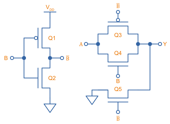
8 Transistor PTL XOR Gate
Above we showed how complex a XOR gate is to build in CMOS logic (12 transistors!). PTL logic can significantly reduce the transistor count for a XOR gate. One such implementation is11:
To see how this works, ignore the simple CMOS inverters on the left and focus on the PTL logic on the right. Input controls which transmission gate is on and which is off. If is LOW, the bottom transmission gate is on and the top is off, passing to the output. Thus:
- If and , then
- If and , then
If is HIGH the opposite happens, the top transmission gate is on and the bottom is off, passing to the output. Thus:
- If and , then
- If and , then
Now it should be pretty easy now to see that this gives you a XOR gate!
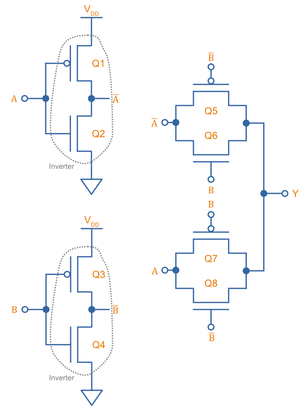
6 Transistor PTL XOR Gate
However, we can reduce the transistor count even further! This following clever circuit implements a XOR gate in PTL logic using a total of only 6 transistors12.
The left-side of the circuit is an “inverter” (but with the MOSFET source leads connected to rather than the rails), and the right-hand side is a transmission gate.
- When , both MOSFETs in the inverter will always be
OFFbecause the gate-source voltage of the N-channel MOSFET can never be more positive than and the gate-source voltage of the P-channel can never be more negative than . The right-hand side transmission gate will be ON, and so the output will equal . - When , the transmission gate will be
OFF, and the inverter will become active, passing through the inverse of to the output.
This makes a XOR gate! Have a play around with the interactive simulation of it below:
Logic Gate Part Numbers
Texas Instruments introduced the SN74xx series of logic ICs in the 1960s, using TTL logic. These parts became very popular and many other manufacturers began making pin-compatible parts. They kept the 74xx section of the part number to aid identification, and hence the 74xx is somewhat standardized across the industry.
The 5400 series is the military rated version of the 7400 series. The 4000 series is the newer CMOS alternative to the 7400 TTL logic. However (and which is somewhat confusing), newer 7400 parts can also be made using CMOS logic, for example, the 74HC4051 analogue multiplexer13. These parts commonly use the logic subfamily names HC or HCT.
Part number descriptions for the popular TTL 74xx family of ICs:
| Part Number | Description | Num. Units | Input | Output |
|---|---|---|---|---|
| 74x00 | Quad 2-input NAND gate | 4 | Normal | Push-pull |
| 74x01 | Quad 2-input NAND gate | 4 | Normal | Open-collector |
| 74x02 | Quad 2-input NOR gate | 4 | Normal | Push-pull |
| 74x03 | Quad 2-input NAND gate | 4 | Normal | Open-collector |
| 74x04 | Hex inverter gate | 6 | Normal | Push-pull |
| 74x05 | Hex inverter gate | 6 | Normal | Open-collector |
| 74x06 | Hex inverter gate | 6 | Normal | Open-collector, 30V/40mA |
| 74x07 | Hex buffer gate | 6 | Normal | Open-collector, 30V/40mA |
| 74x08 | Quad 2-input AND gate | 4 | Normal | Push-pull |
| 74x09 | Quad 2-input AND gate | 4 | Normal | Open-collector |
| 74x10 | Triple 3-input NAND gate | 3 | Normal | Push-pull |
| 74x11 | Triple 3-input AND gate | 3 | Normal | Push-pull |
| 74x12 | Triple 3-input NAND gate | 3 | Normal | Open-collector |
| 74x13 | Dual 4-input NAND gate | 2 | Schmitt trigger | Push-pull |
| 74x4051 | High-speed 8-channel analog multiplexer/demultiplexer | 1 | Analog | Analog |
| 74x4052 | Dual 4-channel analog multiplexer/demultiplexer | 2 | Analog | Analog |
| 74x4053 | Triple 2-channel analog multiplexer/demultiplexer | 3 | Analog | Analog |
The x is a placeholder for the logic subfamily. For example, in 74LSxx the LS represent the low-power Schottky subfamily.
A company specific prefix may be added to the above part numbers depending on the manufacturer.
| Prefix | Company |
|---|---|
| <none> | Nexperia, Philips |
| CD | Texas Instruments |
| DM | National Semiconductor |
| ID | IDT |
| M | STMicroelectronics |
| MC | OnSemi |
| MM | National Semiconductor |
| NLV | OnSemi |
| SN | Texas Instruments |
| TC | Toshiba |
Karnaugh Maps
Karnaugh maps are a way of simplifying combinational logic, often used before realising a combination equation into a number of gates to reduce the complexity.
Logic Simulators
CEDAR Logic Simulator is my personal favourite. Free, easy to use, colours the wires depending on their state, and allows for named nets as well as direct connections.
Example Logic Circuits
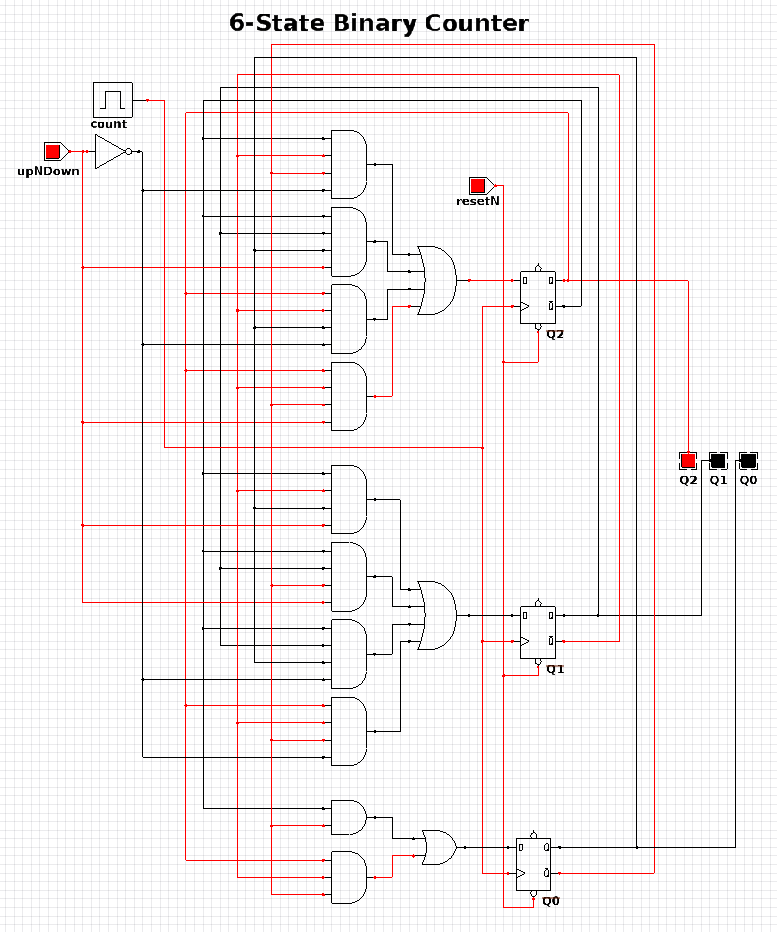
6-State Binary Counter
Category: Counter
Expression Style: Sum of Products
No. of Gates: 14
No. of Flip-flops: 3
1-Bit Inputs: 2 + reset
1-Bit Outputs: 3
Tested On:
- Simulation: Yes (CEDAR Logic Simulator)
- Hardware: Yes
Downloads: CEDAR Logic Simulator File
The 6-state binary counter is a counter which counts from 000 to 101 in the normal binary fashion before resetting back to 0. The output increments on every rising-edge of the count pulse, and the direction pin (upNDown) determines the count direction (when upNDown = 1, the counter goes from 000 to 101, when upNDown is 0 the counter goes from 101 to 000).
The flip-flop equations expressed as sums of products are:
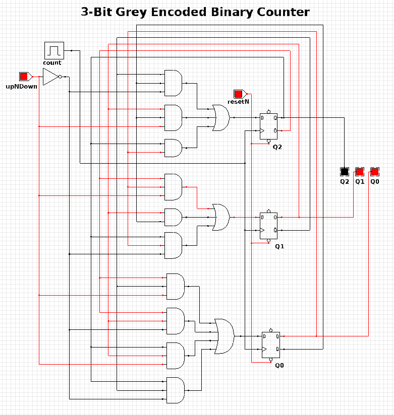
3-Bit Gray Encoded Counter
Category: Counter
Expression Style: Sum of Products
No. of Gates: 14
No. of Flip-flops: 3
1-Bit Inputs: 2 + reset
1-Bit Outputs: 3
Tested On:
- Simulation: Yes (CEDAR Logic Simulator)
- Hardware: Yes
Download: CEDAR Logic Simulator File
The 3-Bit Gray Encoded Counter is a counter that counts from 0 to 7 in binary in a Gray encoded fashion. The counter increments on every rising edge of the bit ‘count’ and the direction bit ‘upNDown’ determines the direction of counting.
Footnotes
-
Wikipedia (2005, Aug 20). List of logic symbols. Retrieved 2021-10-25, from https://en.wikipedia.org/wiki/List_of_logic_symbols. ↩ ↩2
-
McAllister, Willy (2021). Digital logic gates. Spinning Numbers. Retrieved 2021-10-24, from https://spinningnumbers.org/a/logic-gates.html. ↩ ↩2
-
Maxim Integrated (2020). Glossary Definition For XOR Gate. Retrieved 2021-10-22, from https://www.maximintegrated.com/en/glossary/definitions.mvp/term/XOR%20Gate/gpk/1202. ↩
-
Wikipedia (2024, Aug 2). Apollo Guidance Computer. Retrieved 2024-08-21, from https://en.wikipedia.org/wiki/Apollo_Guidance_Computer. ↩
-
Wikipedia (2023, Apr 22). Transistor–transistor logic. Retrieved 2023-05-10, from https://en.wikipedia.org/wiki/Transistor%E2%80%93transistor_logic. ↩
-
Wikipedia (2023, Mar 12). NMOS Logic. Retrieved 2023-04-29, from https://en.wikipedia.org/wiki/NMOS_logic. ↩
-
Wikipedia (2023, Feb 17). CMOS. Retrieved 2023-04-29, from https://en.wikipedia.org/wiki/CMOS. ↩
-
Wikipedia (2023, Mar 20). XOR gate. Retrieved 2023-05-05, from https://en.wikipedia.org/wiki/XOR_gate. ↩
-
University of Utah: John and Marcia Price College of Engineering. ECE/CS 5710/6710 – Digital VLSI Design: Lab Assignment #3. Retrieved 2023-04-24, from https://my.eng.utah.edu/~kstevens/5710/lab3.pdf. ↩
-
Wikipedia (2022, Nov 22). Pass transistor logic. Retrieved 2023-05-05, from https://en.wikipedia.org/wiki/Pass_transistor_logic. ↩
-
Robert Keim (2018, Dec 26). Digital Design with Pass-Transistor Logic. All About Circuits. Retrieved 2023-05-09, from https://www.allaboutcircuits.com/technical-articles/digital-design-with-pass-transistor-logic/. ↩
-
University of Waterloo - ECE. ECE 637 - Lecture 11 - Pass-Transistor Logic. Retrieved 2023-05-09, from https://ece.uwaterloo.ca/~mhanis/ece637/lecture11.pdf. ↩ ↩2
-
Texas Instruments (1997, Nov). CDx4HC405x, CDx4HCT405x High-Speed CMOS Logic Analog Multiplexers and Demultiplexers [datasheet]. Retrieved 2021-10-20, from https://www.ti.com/lit/ds/symlink/cd74hc4051.pdf. ↩