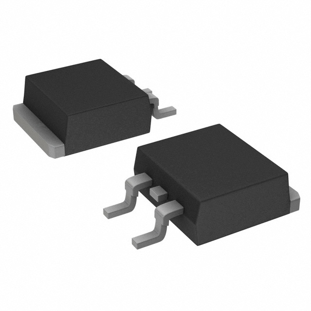
TO-263 Component Package

The TO-263 (Transistor Outline 263, JEDEC) is a large SMD component package. It can be considered the SMD version of the TO-220AB package. It is a 3, 5 or 7 leaded heavy-duty SMD package that allows for good heat-sinking due to a large pad on it’s underside. It is used frequently for high power MOSFETs, LDOs and SMPS.
Synonyms:
- D2PAK (Double Decawatt package)
- DDPAK (Double Decawatt package)
- SMD-220 (named so because the TO-263 is the SMD equivalent of the TO-220).
- TO-263 (Transistor Outline 263, JEDEC)
- TO-263AB (TO-263-3S only)
- TO-279 (TO-263 THIN only, by Texas Instruments)
The height of all TO-263 variants except TO-263 THIN is 4.57mm. TO-263 THIN is 2.00mm high.
For every variant with a different number of pins, there is also an S variant in where the middle lead is cut off.
Solderability: Easy to solder by hand, as long as you have a decent powered soldering iron for the central thermal pad. Easy to solder with infrared and reflow techniques.
Similar To:
TO-263-3/TO-263-3S
The TO-263-3 is the 3-pin variant of the TO-263. TO-263-3S is the same as TO-263-3 except the middle lead is cut off.
Pitch: 2.54mm
The junction-to-ambient thermal resistance for the TO-263-3 component package on both standard JEDEC 2-layer and 4-layer boards is shown below:
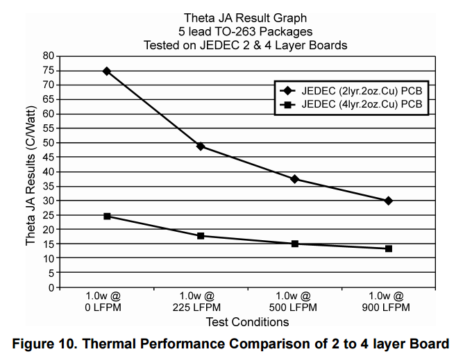
- (1 square inch of copper surrounding pads, connected to ground)
- (copper filling package land-area)
- (pads only, no copper fill)
3D models:
Common Uses:
- High power MOSFETs
- High power LDOs
- High power SMPS (usually with integrated switching element)
TO-263-5
The TO-263-5 is the 5-pin variant of the TO-263.
Thermal resistance of the TO-263-5L THIN:
(no air flow, on JEDEC 4-layer test board)
3D models:
TO-263-7
The TO-263-7 is the 7-pin variant of the TO-263.
Pitch: 1.7mm
3D models:
TO-263 THIN
TO-263 THIN is a variant of the TO-263 component package by Texas Instruments. It shares a similar PCB footprint, but is significantly smaller in height (i.e. thinner).
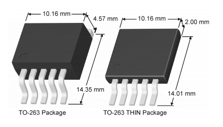
It still has a similar exposed pad on it’s underside (making it footprint compatible with the standard TO-263 package).
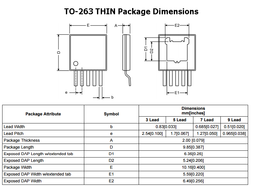
The exact dimensions of the TO-263 THIN package are shown below:
Similar To
The TO-263 is similar to:
- TO-252 (DPAK): The TO-252 (DPAK) is the next step down in power dissipation from the TO-263 (D2PAK) package.
- TO-268 (D3PAK): The TO-268 (D3PAK) is the next step up in power dissipation from the TO-263 (D2PAK) package.