SPI Communication Protocol

SPI (Serial Peripheral Interface) is a communication protocol commonly used to talk between microcontrollers/FPGAs and peripheral ICs on circuit boards. The SPI protocol was initially developed by Motorola. It is full-duplex (data can be sent in both directions at once), and is ideally suited to sending medium-speed data streams (typical rates up to 10-24Mbps1) between devices on the same PCB. It is a de-facto standard, which means there is no governing body that defines and regulates the protocol. This means there are quite a number of protocol variants.
Advantages
- SPI has much higher throughput compared to other board-level communication protocols (such as I2C or 1-wire), primarily because the bus lines are driven both high and low, and there is a separate wire for transmit and receive (full-duplex). However not as fast as protocols such as LVDS.
- SPI can have an arbitrary data/frame length.
- Most logic analysers support SPI decoding.
Disadvantages
- When configured in the standard manner, SPI requires 1 extra control line (for the slave select signal) from the master for every extra slave added to the SPI bus. This can take up more space and I/O pins for designs with a large number of SPI devices.
Physical Layer
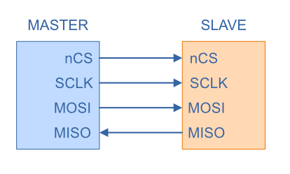
SPI consists of a basis of three wires (SCLK, MOSI and MISO), plus one chip select (nCS) wire per slave. In the special case of only one slave, the chip select line can be dropped and the pin pulled permanently low on the slave.
The purpose of these connections is:
| Name | Function |
|---|---|
| nCS | Chip select, a.k.a. slave select (nSS). This is driven low (hence the n) by the master to select a slave. There is a separate chip select line going from the master to each slave. |
| SCLK | Clock. Driven by the master, this provides the clock signal to the slaves to clock data in and out with. The exact polarity and edges that are used depend on the values of CPOL and CPHA. |
| MOSI | Master out, slave in. A.k.a. main out, subnode in. The master drives the line and provides data to the slaves. Only the slave with nCS asserted (low) listens to the data. |
| MISO | Master in, slave out. A.k.a. main in, subnode out. The selected slave can drive this line to send data to the master. |
One limitation with SPI is that the master has to initiate all communication. This can be a problem if the slave has data for the master but the master hasn’t or doesn’t know when to ask for it. If continuous polling is not feasible, designers get around this by also providing a Data Ready line to the master. This is separate from the SPI interface, and usually set to trigger an interrupt to tell the master to request for the data across the SPI interface.
No specific termination is needed on SPI connections. Long connections (many metres or more) and high data rates (>10MHz) may require standard termination procedures to prevent reflections.
Arduino has moved away from master/slave terminology (supported by an OSHWA resolution) and now uses the following controller/peripheral terminology for SPI:2
| Old (Master/Slave) | New (Controller/Peripheral) |
|---|---|
| SS (Slave Select) | CS (Chip Select) |
| SCLK (Serial Clock) | SCK (Serial Clock) |
| MOSI (Master Out, Slave In) | COPI (Controller Out, Peripheral In) |
| MISO (Master In, Slave Out) | CIPO (Controller In, Peripheral Out) |
Protocol
Many microcontrollers support the SPI protocol with dedicated peripheral hardware to perform the low-level functions associated with sending and receiving SPI data. However, SPI can also be bit banged (see below).
The MSB (most significant bit) is typically sent first, and naturally is then the first to be received. However this is not specified by the standard, and occasionally you will encounter SPI devices that expect data LSB first. There is no pre-defined packet format, so there is no overhead added by the SPI protocol. This makes SPI great for fast transmission of arbitrary data streams, but relies on application specific interpretation of the raw bytes.
Chip select normally uses inverse logic (low = chip selected). It usually is used to ‘frame’ a command sequence.
Because the master has to always drive the clock signal, if the slave wants to send data back to the master, the master must know about this and must have some way of knowing how many clock signals to send.
Modes
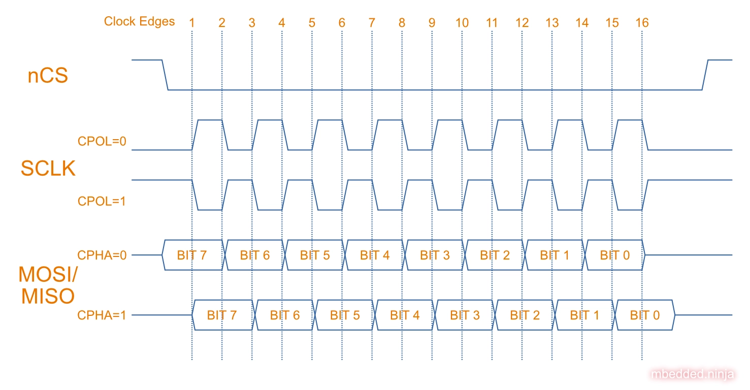
SPI has four standard ‘modes’. These define different polarities of the clock cycle and whether sampling is on the positive or falling edge of the clock. This is sometimes called the SPI Clock Polarity (CPOL) and SPI Clock Phase (CPHA).
The clock polarity (CPOL) determines whether the idle state of the clock signal is either 0 (CPOL = 0) or 1 (CPOL = 1).
The clock phase (CPHA) determines whether data is captured/sent on the rising or falling edge. If CPHA = 0, then data is sampled on the first clock edge. If CPHA = 1, then data is sampled on the second clock edge. This is true no matter what the clock polarity (CPOL) is set to, and applies both to the master and all the slaves. Note that if CPHA = 0, then data must be setup before the first clock edge. If CPHA = 1, then the devices have the initial clock edge to shift data onto the lines, in preparation for sampling on the second clock edge.
The following table shows the naming conventions for Microchip PIC or ARM-based microcontrollers, as well as what is used for the Arduino SPI API:2
| SPI Mode | Clock Polarity (CPOL) | Clock Phase (CPHA) | Which Clock Edge Is Used To Sample/Shift? |
|---|---|---|---|
| 0 | 0 | 0 | Data sampled on rising edge and shifted out on falling edge. |
| 1 | 0 | 1 | Data sampled on falling edge and shifted out on rising edge. |
| 2 | 1 | 0 | Data sampled on falling edge and shifted out on rising edge. |
| 3 | 1 | 1 | Data sampled on rising edge and shifted out on falling edge. |
A common point of confusion is what clock phase (CPHA) means for data sampling/shifting for the different clock polarities. I have seen many sites and diagrams online which state that a clock phase CPHA of 0 means that data is sampled on the rising edge (this is only true if CPOL is also 0).
The following diagram gives a graphical representation of the different CPOL and CPHA settings. Bits on the MOSI and MISO lines are always sampled half-way between the transitions. For CPHA=0 this means data is sampled on clock edges 1, 3, 5, etc. and for CPHA=1 data is sampled on clock edges 2, 4, 6, etc.
Below shows an example of a single-byte transfer with CPOL=0 and CPHA=0. The master sends the data 0xA1 and the slave sends 0x75. Data is sampled at the dotted red vertical lines.
And now for comparison, let’s see what it would look like if we transmitted the same data but with CPOL=1 and CPHA=1 (Mode 3):
The standard defines these different modes to allow for greater variability in the master and slave devices that can use SPI.
To give you an example of what it means for firmware, below is a screenshot of the SPI modes table from the Microchip SAM D21 MCU datasheet. We are lucky in this case, the SAMD21 microcontroller supports all four modes of operation.
Can A Single Master Support Multiple SPI Modes On The Same Bus?
Yes, a single master can support different SPI modes on the same bus, as long as the master can be configured to all the relevant modes (most SPI peripherals inside microcontrollers support multiple SPI modes). The SPI slaves do not care what happens on the SCLK, MOSI and MISO lines while their chip select is inactive (high). So other slave devices that use other SPI modes can be communicated with whilst the chip select is held high for all other slave devices (as per normal operation). Care must be taken to change the clock polarity to what the slave node expects before making its chip select active.
Timing
SPI is inherently synchronous (requires a clock signal). There is no such thing as asynchronous SPI, as there is with UART and other transmission protocols.
Bit Banging
Bit banging (on the master device) can be easily done with SPI since it is synchronous and the master has full control over the clock, hence the timing can be manipulated. Care has to be taken to assert the right lines and read data before applying the next clock transition, as well as obeying any minimum/maximum time specifications for each state.
Daisy-Chaining
SPI daisy-chaining is way of overcoming the routing/capability issue of having many SPI slaves and therefore many slave select lines. ICs have to support SPI daisy-chaining with a DOUT (or similar) signal before you can implement it.
The basic idea is that instead of data line being connected to every slave, the master’s data line is connected to one slave only, and that slave’s DOUT is connected to the next slave’s data in, forming a “daisy chain”. The other difference is that a single chip select line is routed to all slave ICs.
The data is passed from the microcontroller to the first slave, who stores it in a shift register. After a number of clock cycles, the data reaches the end of its internal shift-register, and is passed onto the next slave. The microcontroller continues passing out data until all the slaves’ shift-registers are full, at which point a pulse is sent down the global chip select signal, which causes the slave devices to read/execute/do whatever with the data currently in its shift register.
Some devices that support daisy chaining are Microchip’s MCP42xxx digital potentiometers and Analog Devices’ (formerly Linear Technology) LED drivers.
Point-to-Point SPI
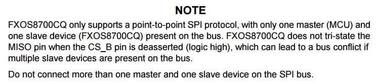
Some slave devices only support point-to-point SPI communication. This means that there can only be one master on the bus, and also only one slave (the device which supports point-to-point SPI). The Freescale (now NXP) FXOS8700CQ magnetometer is one such example.
Dedicated Chip Select Pins
Some microcontrollers have dedicated chip select pins which are connected to the SPI peripheral inside the microcontroller. This pin usually has a number of different purposes:
- Used to select a slave device for communication (only really works when the SPI bus has only 1 slave on it)
- Synchronize data frames
- Detect conflicts between multiple masters
On STM32 microcontrollers this pin is called NSS (which stands for not slave select, the not denoting that the signal is active low).
Shared MOSI/MISO Pins
Some low-pin count packaged ICs use shared MOSI/MISO lines. One such example is some of the DPOTs in the Microchip MCP4XXX family. The 8-pin potentiometer variants such as the MCP4131 contain a single MOSI/MISO pin (called SDI/SDO). This obviously prevents data from being transmitted in both directions at the same time. If connecting such a device up to a normal hardware SPI peripheral, a resistor is needed to prevent driver contention (as shown in the below image) when the MCP4131 sends data back to the microcontroller. If you are bit-banging the SPI communications, you can smartly turn the host controller output into an input at the right clock edge to receive data and eliminate the need for the resistor.
The datasheet says exactly when the SDI will be turned into an SDO and data sent back:
The 8-lead Single Potentiometer devices are pin limited so the SDO pin is multiplexed with the SDI pin (SDI/SDO pin). After the Address/Command (first 6-bits) are received, If a valid Read command has been requested, the SDO pin starts driving the requested read data onto the SDI/SDO pin.5
Dual And Quad SPI
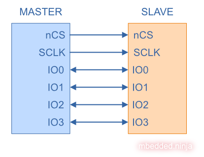
Dual and Quad SPI (QSPI) are extensions on the basic SPI bus which allow for faster communication rates. Dual SPI replaces the MOSI and MISO lines with bi-directional IO0 and IO1 lines. This allows twice the data transfer rate in any one direction at a time, however, it now makes the protocol half-duplex (it is now unable to transfer data in both directions at the same time).
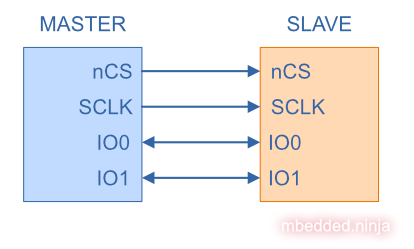
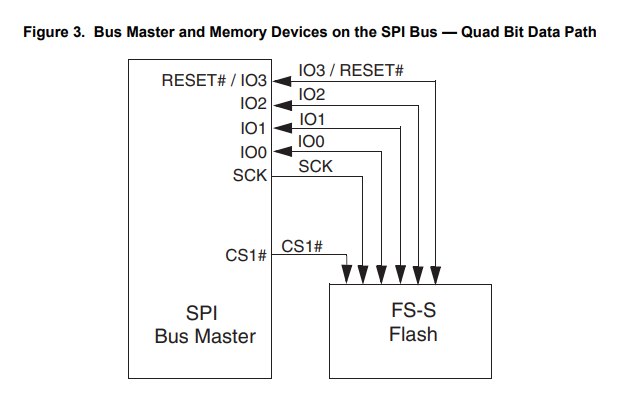
QSPI takes this idea even further and adds two additional bi-directional data lines, IO2 and IO3, as shown in the following diagram:
With the four data lines in QSPI, a single byte can be sent in two clock cycles (4 bits per clock cycle). QSPI is commonly used for external NOR flash memory. Examples include the Cypress S79FS01GS 1 Gbit, 1.8 V Dual-Quad Serial Peripheral Interface with Multi-I/O Flash. Chips that support QSPI usually also support Dual SPI.
Octo-SPI and Hexadeca-SPI
Even dual and quad SPI have not been fast enough for some users, and as a result there is now Octo-SPI (8 lines) and Hexadeca-SPI (16 lines, abbreviated HSPI). These are extensions of the SPI bus in the same way dual and quad SPI were, they give up the full-duplex comms for half-duplex and add more data lines for faster transfers. Octo-SPI almost always runs using DDR (double data rate) when interfacing with memory. This gives data on both edges of the clock. Octo- and Hexadeca-SPI are used for fast external memory interfaces (e.g. PSRAM, HyperRAM, HyperFlash). It is fast enough to allow for XIP (execute-in-place — instructions are executed directly from external memory rather than being copied into internal memory first).
STMicroelectronics MCU families such as STM32L4, L5, H5, H7, N6, U3, and U5 support this bus.7 STMicroelectronics originally started with a OCTOSPI peripheral which supported Octo-SPI. They then superseded this with the XSPI peripheral which can do both 8-bit and 16-bit width transfers. This peripheral supports SDR, DDR, classic SPI-flash command mode, HyperBus and the JEDEC xSPI profile.
Execute-In-Place (XIP)
Many QSPI flash ICs support execute-in-place (XIP). This is when a section of the CPUs main memory is mapped to the external flash memory. The CPU is unaware that this section of memory is off-chip, and the fetching process happens automatically in the background over a QSPI interface.
Firmware
The Arduino platform provides a consistent API for accessing peripherals on an SPI bus. The API is accessed by including SPI.h in your .cpp file. If the microcontroller has only one SPI bus, it can usually be accessed via the global SPI.
#include <SPI.h>
const int slavePin = 20;
int main() {    uint8_t val1, val2;
    // Begin SPI transaction, setting clock speed to 1MHz, most significant bit first (typical), and    // SPI Mode 0 (CPOL=0, CPHA=0).    SPI.beginTransaction(SPISettings(1000000, MSBFIRST, SPI_MODE0));
    // Assert the slaves chip select (drive low)    digitalWrite(slavePin, LOW);
    // Two bytes transferred across, and read the two bytes sent back to us    val1 = SPI.transfer(0xA1);    val2 = SPI.transfer(0x07);
    // De-assert the chip select    digitalWrite(slavePin, HIGH);
    // End transaction, SPI bus is now free to be used by other devices    SPI.endTransaction();}
SPI in Low Power Design
Some SPI slaves will be explicitly designed for low power operation and provide low power modes of operation. Make sure that all SPI digital inputs are in valid logic states (HIGH or LOW) during sleep, otherwise the input buffers will draw current due to shoot-through current (which can be typically 50-1000uA).
This includes the lines from the master to the slave (SCK and MOSI, these are inputs w.r.t. to the slave) and from the slave to the master (MISO, this is an input w.r.t. to the master). The slave(s) will not typically drive the MISO line during sleep, so make sure you connect a high valued (e.g. 100kΩ to 1MΩ) pull-down or pull-up resistor to the MISO line to keep it in a valid logic state during sleep.
More information on this can be found in the low power design page.
Non-Standard Uses
WS2812 RGB LEDs
Microcontroller SPI peripherals are commonly used to generate the data to talk to long strings of WS2812 RGB LEDs. The WS2812 RGB LEDs feature a custom 1-wire communications protocol. There is no clock line, only a single data line. Each bit is a fixed width, and a 0 is communicated with the line staying HIGH for a particular amount of time during the bit, and then transitioning low. A 1 is communicated by the voltage staying HIGH for slightly longer during the bit before transitioning to 0. This “return to zero (RTZ)” scheme allows the clock to be easily recovered from the data.
Depending on the MCU, generating these timings by “bit-banging” could be difficult because of the fast baud rate and HIGH/LOW timing requirements. However, an SPI peripheral running at a faster bit rate can be used to generate the data relatively easily. One option is to set the SPI speed so there are three SPI bits for every WS2812 bit. The SPI bit period can be set to 0.4us, so that three bits takes 1.2us. Then you can send the SPI bit pattern 100 for a WS2812 0 and a 110 for a WS2812 19. Using 8 SPI bits per WS2812 bit is another approach.10
In all of these cases, only the MOSI output on the SPI peripheral is used. SCLK and MISO are not used.
Similar Protocols
Microwire (uWire)
The Microwire protocol is older than the SPI protocol, and began life as a protocol used by National Semiconductors in their COPS processor family.11 It is generally equivalent to SPI when CPOL = 0 and CPHA = 0.12 The wires are called SO, SI and SK.13
mSPI (mini-SPI)
The mSPI bus is a modification of the SPI bus that enforces that the comms protocol always has 4-wires, no matter how many slave devices are attached. This simplifies the software needed on the slave devices. All devices share the same SS (slave select) line.
RapidS
The RapidS term is used by Atmel and Adesto Technologies. It is commonly present on memory chips such as EEPROM and Flash memory ICs. The RapidS serial interface is SPI compatible for frequencies up to 33MHz. The RapidS protocol is different to the Rapid8 protocol, which is a parallel interface.
Footnotes
-
Kathleen Chan. What are the Differences of Single vs Dual vs Quad SPI?. TotalPhase. Retrieved 2022-06-25, from https://www.totalphase.com/blog/2020/05/what-are-the-differences-of-single-vs-dual-vs-quad-spi/. ↩
-
Arduino. Arduino & Serial Peripheral Interface (SPI). Retrieved 2022-06-25, from https://docs.arduino.cc/learn/communication/spi. ↩ ↩2
-
Microchip (2021). SAM D21/DA1 Family: Low-Power, 32-bit Cortex-M0+ MCU with Advanced Analog and PWM (datasheet). Retrieved 2022-10-10, from https://ww1.microchip.com/downloads/en/DeviceDoc/SAM-D21-DA1-Family-Data-Sheet-DS40001882H.pdf. ↩
-
NXP (2017, Apr 25). FXOS8700CQ 6-axis sensor with integrated linear accelerometer and magnetometer. Retrieved 2022-06-02, from https://www.nxp.com/docs/en/data-sheet/FXOS8700CQ.pdf. ↩
-
Microchip (2008). Microchip MCP413X/415X/423X/425X: 7/8-Bit Single/Dual SPI Digital POT with Volatile Memory (datasheet). Retrieved 2022-06-02, from https://ww1.microchip.com/downloads/aemDocuments/documents/OTH/ProductDocuments/DataSheets/22060b.pdf. ↩ ↩2
-
Infineon (2019, Nov 22). S25FS128S/S25FS256S: 1.8 V, Serial Peripheral Interface with Multi-I/O, MirrorBit® Non-Volatile Flash (datasheet). Retrieved 2022-06-26, from https://www.infineon.com/dgdl/Infineon-S25FS128S_S25FS256S_1.8_V_Serial_Peripheral_Interface_with_Multi-I_O_MirrorBit(R)_Non-Volatile_Flash-DataSheet-v14_00-EN.pdf?fileId=8ac78c8c7d0d8da4017d0ed6b5ab5758. ↩
-
STMicroelectronics. AN5050: Getting started with Octo-SPI / Hexadeca-SPI and XSPI interface on STM32 MCUs [application note]. Retrieved 2026-06-09, from https://www.st.com/resource/en/application_note/an5050-getting-started-with-octospi-hexadecaspi-and-xspi-interface-on-stm32-mcus-stmicroelectronics.pdf. ↩
-
Worldsemi. WS2812B - Intelligent control LED integrated light source [datasheet]. Adafruit. Retrieved 2024-01-15, from https://cdn-shop.adafruit.com/datasheets/WS2812B.pdf. ↩
-
Controllerstech. WS2812 LEDs using SPI. Retrieved 2024-01-15, from https://controllerstech.com/ws2812-leds-using-spi/. ↩
-
Rudra Lad. NeoPixel WS2812b SPI driver with Ada on STM32F4 Discovery. Hackster. Retrieved 2024-01-16, from https://www.hackster.io/RVLAD/neopixel-ws2812b-spi-driver-with-ada-on-stm32f4-discovery-d330ea. ↩
-
ScienceProg. Microwire compared to SPI and I2C. Retrieved 2022-06-02, from https://scienceprog.com/microwire-compared-to-spi-and-i2c/. ↩
-
Microchip Forum (2006, Nov 13). Differences between SPI, 3-Wire and Microwire. Retrieved 2022-06-02, from https://www.microchip.com/forums/m202051.aspx. ↩
-
Texas Instruments (1992, Jan). AN-452: MICROWIRE Serial Interface. Retrieved 2022-06-02, from https://www.ti.com/lit/an/snoa743/snoa743.pdf. ↩