

 NinjaCalc
BGA Component Package

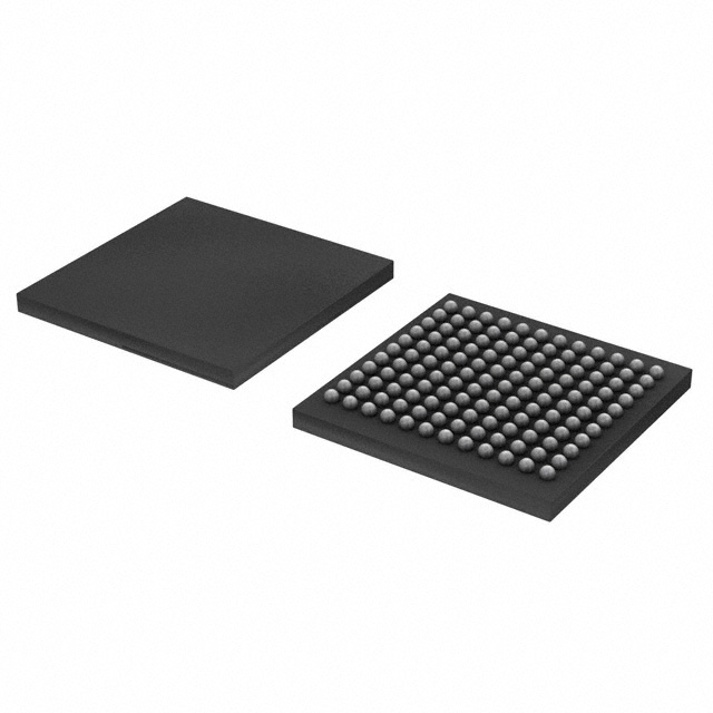
BGA (Ball Grid Array) is a high-density SMD component package which can have from 4 to several thousand pins. Common pitches are 0.5mm, 0.8mm, and 1.0mm. BGA packages are used to either make components very small or to encompass a large number of leads. Large modern FPGAs and CPUs have several thousand balls!
BGA usually requires a reflow oven, infrared heater or hot-air rework station to solder. Expert-level solderers can use the “dead-bug” prototyping method and attach super-thin wires to each ball when the package is upside down, but do not consider this a reliable or fast method! Because the solder joints are hidden underneath the package, X-ray inspection is usually needed to verify that all of the balls have correctly soldered onto the pads (electrical testing can find opens and shorts, and the outer rows can be viewed from the side with optical inspection, but only X-ray lets you see every joint). See The PCB Rework Guide for more information on reworking PCBs.
During reflow, the surface tension of the molten solder pulls the package into alignment with the pads, so BGAs are quite tolerant of small placement errors.
Common uses include:
- Microcontrollers
- FPGAs
- High-density SMD ICs
- CPUs
- GPUs
- Memory
Similar To
Ball Layout
A particular BGA package may not have a complete grid of balls. BGA packages also come in a straight or staggered ball layout.
Ball Numbering
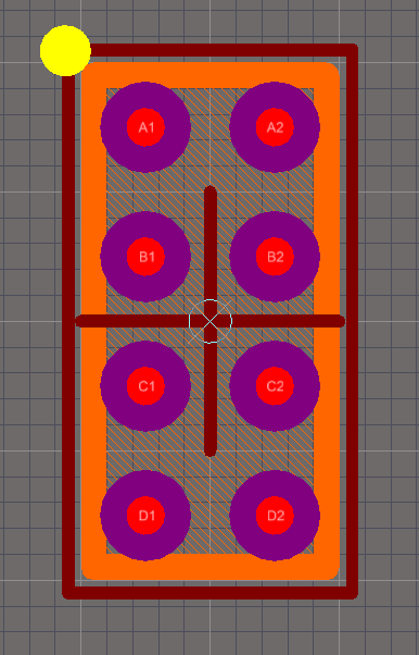
BGA balls are identified by a row letter and a column number, e.g. A1, C3, D11. Ball A1 is in the corner marked by the pin 1 indicator on the package. By JEDEC convention, the letters I, O, Q, S, X and Z are skipped as they are easily confused with numbers or other letters. Packages with more rows than there are letters continue with double letters (AA, AB, …).
BGA Pad Diameter
The pad diameter for a BGA footprint can be determined by one of three methods:
- Maximum material condition (MMC)
- Least material condition (LMC)
- Percentage reduction of nominal ball diameter (e.g. 20%)
Soldermask Considerations
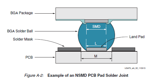
There are two ways of defining the solderable area of a BGA pad on the PCB:
- SMD (soldermask defined): The copper pad is larger than the soldermask opening, so the soldermask overlaps the edge of the copper and defines the solderable area.
- NSMD (non-soldermask defined): The soldermask opening is larger than the copper pad, so the copper itself defines the solderable area.
NSMD pads are generally preferred for BGAs. The size of the copper is more tightly controlled by the etch process than the soldermask is by its registration, and NSMD pads avoid the stress concentration point where the soldermask overlaps the pad.1 NSMD pads should also be used when vias are placed in the pads.1
Fan-out
Routing signals out from the inner balls of a BGA is called fan-out. For coarser pitches (e.g. 0.8mm and up), the common approach is the dog-bone fan-out, where a short track connects each pad to a via placed in the gap between four balls. For finer pitches there isn’t enough room for this, and via-in-pad (usually with microvias) is used instead, where the via is placed directly in the BGA pad.
Variants
- CABGA (Chip Array BGA)
- CTBGA (Thin Chip Array BGA)
- DSBGA (Die-Size BGA): Used by Texas Instruments. JEDEC standard MO-207. See below for more info.
- FBGA (Fine-pitch BGA): Many manufacturers also assign their own package codes, e.g. the Xilinx FGG484 is a 484-ball, Pb-free fine-pitch BGA.
- FCBGA (Flip-Chip BGA): The die is flipped and bonded directly to the package substrate. Commonly used for high-performance ICs such as CPUs, GPUs, FPGAs and TI’s mmWave radar ICs.
- X-DSBGA (Very thin die-size BGA). JEDEC standard MO-211-C.
- xDSB (Square and rectangular die-size BGA). JEDEC standard MO-207N.
DSBGA
DSBGA (Die-Size BGA) is the name given by Texas Instruments for their family of BGA packages where the die size is the same as the package size. They are also known by the term Wafer-Level Chip Scale Package (WLCSP). As of December 2019, they are available in 0.30, 0.35, 0.40, and 0.50mm pitches.1
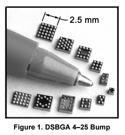
Texas Instruments also assigns a package code to each package within the DSBGA family. Here are some examples (this is in no way an exhaustive list):
| TI Package Code | Description |
|---|---|
| YDC | DSBGA, 4 Leads, Pitch 0.5mm, Body 1.1 × 1.1mm, Height 0.4mm |
| YEA | DSBGA, 5 Leads, Pitch 0.5mm, Body 0.9 × 1.4mm, Height 0.5mm |
| YEB | DSBGA, 4 Leads, Pitch 0.5mm, Body 1.3 × 1.3mm, Height 0.625mm |
| YEC | DSBGA, 6 Leads, Pitch 0.5mm, Body 1.8 × 1.3mm, Height 0.625mm |
| YZP | DSBGA, 8 Leads, Pitch 0.5mm, Body 1.9 × 0.9mm, Height 0.5mm |
Note that confusingly, the three-letter Texas Instruments code is not unique for a particular package. For example, the code “YZP” may refer to a 5, 6, or 8 ball DSBGA package, which also may have different height, width and length dimensions.
Footnotes
-
Texas Instruments (2019, Dec). AN-1112 DSBGA Wafer Level Chip Scale Package (Rev. AI) [application note]. Retrieved 2026-10-29, from https://www.ti.com/lit/an/snva009ag/snva009ag.pdf. ↩ ↩2 ↩3
-
AMD/Xilinx (2024, Mar 13). UG475: 7 Series FPGAs Packaging and Pinout Product Specification (v1.20) [product specification]. Retrieved 2026-10-29, from https://docs.amd.com/v/u/en-US/ug475_7Series_Pkg_Pinout. ↩