Analogue Switches (Transmission Gates)

Analogue switches are electrical circuits which connect and disconnect analogue signals. When used in digital circuits (e.g. flip-flops) the same circuit made below from MOSFETs is normally called a transmission gate.
Apart from the fact that analogue switches work with continuous voltages and digital buffers only work with discrete HIGHs or LOWs, one other big difference is that analogue switches allow bi-directional data flow, whilst digital buffers only allow uni-directional data flow. Digital buffers have a dedicated IN and OUT, whilst each side of an analogue switch can either be IN or OUT (IN/OUT).
When many analogue switches are combined so that one analogue signal can be routed to many different locations, it is called an analogue multiplexor. These are discussed on the Multiplexers And Demultiplexers page.
How Do Analogue Switches Work?
CMOS (MOSFETs) is the most popular IC process to make analogue switches from, however JFETs are used for special applications such as video switching due to the high bandwidth and signal quality requirements of the signal1.
The basic idea is to connect 1 N-channel and 1 P-channel MOSFET together in parallel, so their sources and drains are connected together (although because the substrates are not connected to the source, there is symmetry in the construction of the MOSFET and no actual difference between the source and drain, more on this below).

When the analogue switch is turned on, the resistance of each MOSFET depends on the analogue switch voltage. At low voltages, the N-channel MOSFET’s resistance is very low and conducts most of the current. As the voltage rises, the P-channel MOSFET’s resistance decreases whilst the N-channel’s increases, and the P-channel conducts most of the current. The graph below shows the resistance of each individual MOSFET, as well as the combined resistance seen by an external circuit. The combined resistance is the parallel resistance of both the N-channel and P-channel MOSFET.
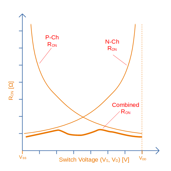
Notice how in the above image the total (combined) resistance is not constant, nor linear! This non-linearity can cause signal degradation depending on the input and output impedances of the circuitry connected to it. Generally speaking, the on resistance of the analogue switch is not an issue if driven from a suitable “stiff” source, and passed through to a high-impedance input such as an ADC (assuming you allow for enough settling time, the input capacitance of the ADC will form a low-pass RC circuit with the switch resistance).
Transmission Gates
A transmission gate (which can be abbreviated to just TG2) is used to describe the same MOSFET-in-parallel circuit as the analog switch above, but when used in a digital context. It is commonly used in the design of latches and flip-flops, and is an integral part of pass transistor logic (PTL).
When showing a transmission gate on a schematic, it is almost never drawn showing discrete MOSFETs. It is usually simplified in the form of a “single bow tie” or “double bow tie” symbol, as shown below. Sometimes, simplified MOSFET symbols are shown, in where no arrows are used to indicate NMOS from PMOS, but rather an “inverting bubble” is added to the gate of the PMOS MOSFET.
is the gate of the N-channel MOSFET, the gate of the P-channel. and are the two sides of the transmission gate.
Notice how the clock signal and its inverse are provided to the gates. This will enable the transmission gate when the clock is HIGH, and disable it when LOW. If you swap and you will invert the logic and instead enable the transmission gate when the clock is LOW. The clock signal is the most common signal provided to turn the transmission gate on and off.
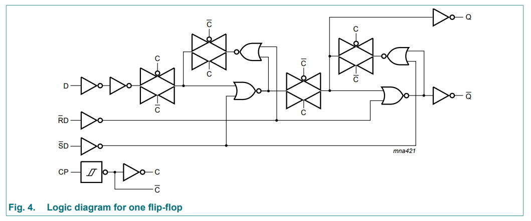
To show a real-world use case for a transmission gate, this is the logic diagram for the Nexperia 74HC74 dual D-type flip-flop IC3:
Crosstalk
For analogue switch ICs with more than one switch, the amount of channel-to-channel crosstalk becomes an important metric. Crosstalk is the unwanted coupling of one analogue signal path to another inside the IC due to parasitic capacitances. Crosstalk is due to:
- The proximity of the other channel traces creating capacitance.
- The capacitance between the pins on the switching MOSFETs inside the IC.
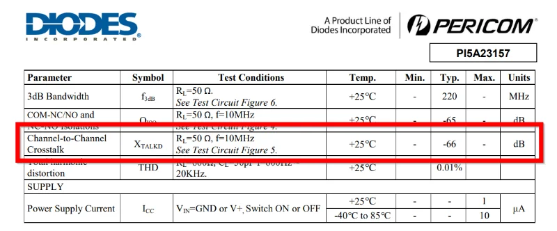
Most analogue switches will specify the amount of cross-talk in dB at a particular frequency. Most are in the -60 to -80 dB range at 10 - 100 MHz. When crosstalk is specified in dB, it uses the following equation:4
where:
- is the voltage of the driven line at the crosstalk test frequency.
- is the voltage measured on the victim line at the crosstalk test frequency.
Both should be measured the same way (both peak, both RMS, etc.) — the dB ratio means the scale cancels.
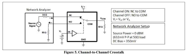
An example of a test circuit used to measure crosstalk is shown below.
Off-Isolation
Off-isolation measures the ability of the analogue switch to block the input from the output when the switch is disconnected (open). It is quoted as a dB-at-a-frequency just like crosstalk, and the two are commonly confused. It has a similar equation to crosstalk:
where:
- is the voltage on the input of a switch node.
- is the voltage on the output of a switch node.
Input signal leaks to the output primarily through the drain-to-source capacitance of the MOSFETs .
Related but not strictly the same thing is power off isolation, which is the ability of the switch to keep the input and output disconnected even when the IC loses supply power to its and pins.
Switching Speeds
For switches with more than one pole, the IC manufacturers usually make sure there is a specified “break-before-make” period.
Power Consumption
The following values are considered a low-power switch:
- = 25nA (typ), 40nA (max)
- = 5nA (typ), 90nA (max)
Examples
Intersil ISL43L410
The Intersil ISL43L410 is a low on-resistance, low-voltage single-supply, DPDT analogue switch. One of its main selling points is its low power consumption with an (typ) and (max). Leakage current is (typ), (max).
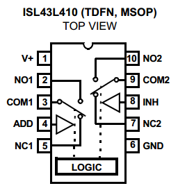
This IC has the nice feature that the common net can be disconnected from both NC and NO at the same time. However, both switches cannot be switched from NC to NO independently, which might be a deal-breaker for some designs.
Maxim DS3690
The Maxim DS3690 (now Analog Devices) is a 26-channel transmission gate in a TQFN-56 package7. Each channel is electrically independent — there’s no signal path between channels — but all 26 share a single control input. It is designed for digital bus isolation when digital bus components are disabled or removed.
Manufacturer and Supplier Links
Footnotes
-
Analog Devices (2008, Oct.). MT-088: Analog Switches and Multiplexers Basics. Retrieved 2021-09-01, from https://www.analog.com/media/en/training-seminars/tutorials/MT-088.pdf. ↩
-
Electronics Tutorials. Transmission Gate. Retrieved 2023-04-22, from https://www.electronics-tutorials.ws/combination/transmission-gate.html. ↩
-
Nexperia (2023, Feb 9). 74HC74; 74HCT74 - Dual D-type flip-flop with set and reset; positive edge-trigger. Retrieved 2023-04-11 from https://assets.nexperia.com/documents/data-sheet/74HC_HCT74.pdf. ↩ ↩2
-
Renesas (1999, Apr 23). AN-18: Switching Analog Signals [application note]. Retrieved 2026-05-28, from https://www.renesas.com/en/document/apn/18-switching-analog-signals. ↩
-
Diodes Incorporated (2022, Mar 10). PI5A23157: Low Voltage Dual SPDT Analog Switch [datasheet]. Retrieved 2026-05-29, from https://www.diodes.com/datasheet/download/PI5A23157.pdf. ↩ ↩2
-
Intersil (2014, Nov 17). ISL43L410: Ultra Low ON-Resistance, Low Voltage, Single Supply, DPDT Analog Switch [datasheet]. Retrieved 2026-05-28, from https://www.mouser.com/catalog/specsheets/intersil_fn6090.pdf. ↩
-
Maxim (2007, Oct). 3.3V 26-Channel, Three-Stateable Transmission Gate. Retrieved 2023-04-22, from https://www.analog.com/media/en/technical-documentation/data-sheets/DS3690T-DS3690TTRL.pdf. ↩ ↩2