The Schematic And PCB Design Guide

Schematic
Component Selection
All other things being equal, try to pick components which come in standard packages and have part alternatives (ideally from different manufacturers). This is especially important when there are long lead times and/or component shortages.
No Ray Guns
Keep positive power rails pointing up, and ground and negative power rails pointing down. No ground symbols lying on their side (affectionately known as ray guns) or upside down!
Add Decoupling Capacitors
As a rule-of-thumb, add 100nF decoupling capacitors to all IC power rails. If the IC’s datasheet has specific decoupling advice, follow that instead.
PCB
Estimating PCB Design Time
A good way of estimating the time to design a PCB board is by working out the utilization ratio. This is the total land area of all components divided by the total surface area of the board. A utilization ratio of 0.25 is easy enough to route, and the board starts getting harder as the ratio hits 0.50 and above. There is a good article, ‘Estimating PCB Design Time And Complexity’, that explains this in more detail, and even has a program to work it out for you.
Copper (Track And Gap) Clearance
The copper to copper and copper width clearance are usually the same value. This is commonly called the ‘Track and Gap’ clearance. Typical Values:
- 0.5mm - Homemade PCBs
- 0.2mm - Professionally printed PCBs
- 0.1mm - High-end PCBs
Copper To Board-Edge Clearance
Typical copper to board-edge clearance : 0.3048mm (12 mil) This is the closest you can put copper to the board edge. This usually accommodates for slight board-misalignment and tool inaccuracies when routing the board into shape so that the router will not cut into the copper and leave ‘exposed copper’ ( a big no-no, usually). However, there are cases in which this rule is ignored, for example when you a making an RF shield or box from pieces of PCB, and need the copper to go right to the edge so that they can be soldered together into a box shape. This clearance is usually larger than the ‘track and gap’ clearance.
One-off Costs
These are sometimes called tooling costs. There is no charge for these if the same PCB design is made again in the future.
For a manufacturer, these costs include:
- Loading the design files into their system
- Checking the PCB for any manufacturing problems and adjusting as necessary (e.g. removing soldermask slivers)
For an assembler, these costs include:
- Loading the design files into their system. This is normally substantially higher than the similar manufacturing costs, as they have to load all of the components into their system
- Sourcing all of the required components (this may also fall under re-occurring costs)
- Manufacturing a soldermask stencil (typically laser cut from stainless steel)
Mounting
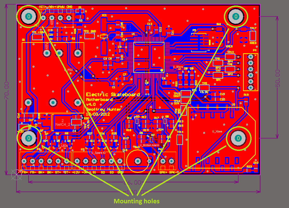
Don’t forget to consider how the PCB is going to be mounted. One of the most common things accidentally left off a PCB. Normally all it requires is four holes (un-plated) in the corners for screwing in bolts/supports or just enough free PCB space to stick on rubber feet. M3 bolts and nuts are commonly used. Remember to consider the implications of using metal bolts next to/on-top of electrical signals. There are nylon bolts and washers when insulation is needed. Loctite (thread-locker) can be good to prevent bolts/screws from undoing. The following picture shows the four mounting holes on a PCB. Notice one is underneath a component (the Xbee module).
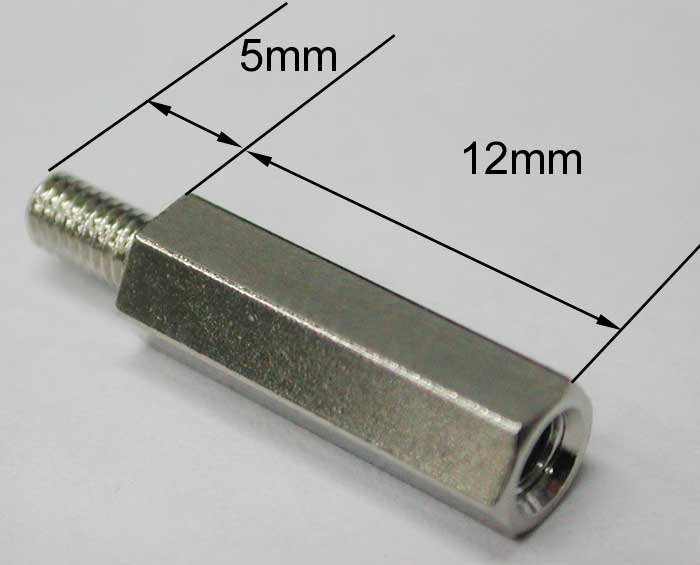
Standoffs are good for providing clearance between the PCB and the mounting surface. You can buy plastic or metallic standoffs for most electronic suppliers, and they come in round or hex shapes. Electrical enclosures usually come with standoffs built into the structure.

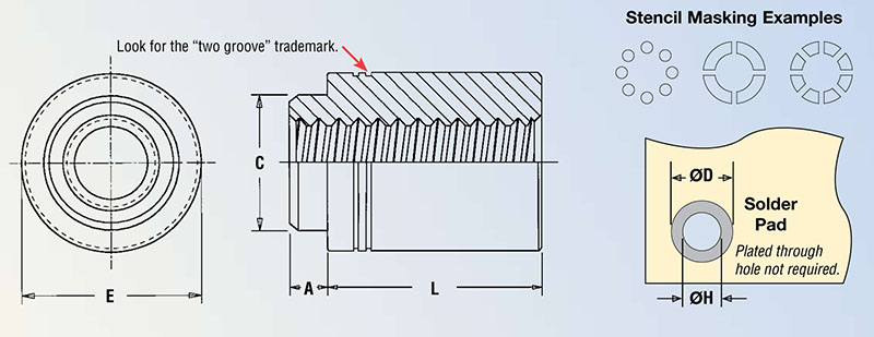
Below is an example of an SMD standoff from PEM Engineering.
Desiccant
Desiccant (a moisture absorbing compound), can be a good thing to use if your PCB is at risk of condensation.
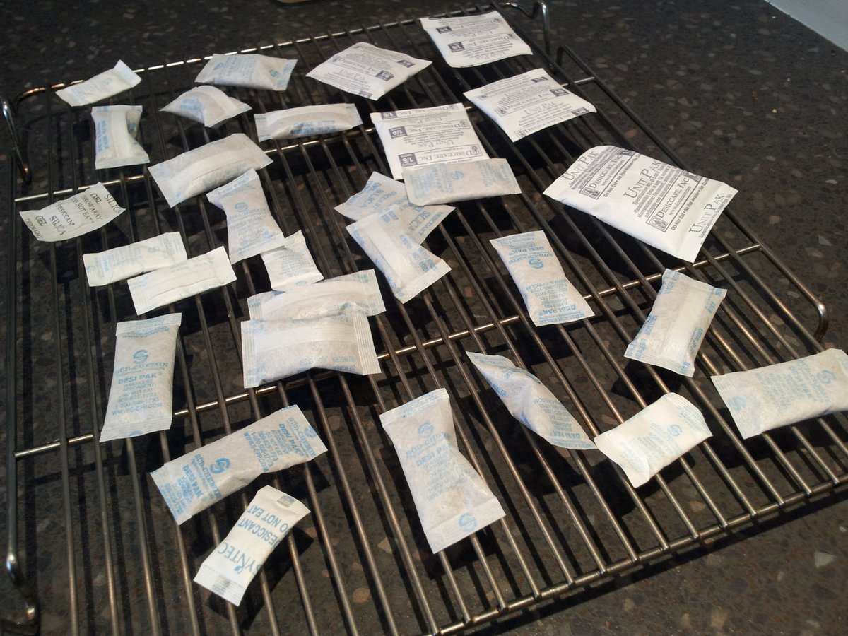
See the Desiccant page for more info.
Making It Look Good
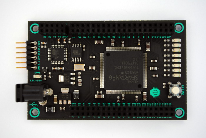
It could be said that PCB design is an art form. Personally, I take great pleasure in making a PCB that got the looks as well as the functionality. And it’s helpful that most steps toward making a PCB look good actually tie in well with good design practises anyway.
This is an example of a PCB which I really like. It is called “The Mojo”, and it is an Arduino-like FPGA development board. I love the black and green colour combination of the soldermask and silkscreen respectively.
Late Cycle Rework
“Late cycle rework” is the term given to PCB reworking done at the late stages, just before being sent off to the PCB manufacturer. Late cycle work is normally a bad thing, it is estimated that work done in this stage costs 10x as much as it does in the earlier stage.
Panelisation
Panelisation is when you combine multiple PCB designs onto one PCB board, with the normal intention of saving costs associated with producing individual PCBs. Most PCB manufacturers support panelisation and will route/v-score each design out for you, so you can separate them easily.
Altium supports panelization. There is also software called GerbMerge, an open-source tool which merges Gerber files together.
Sending It To A PCB Manufacturer
For a review on different PCB manufacturers and their capabilities, see the PCB Manufacturers section of the Electrical Suppliers page.
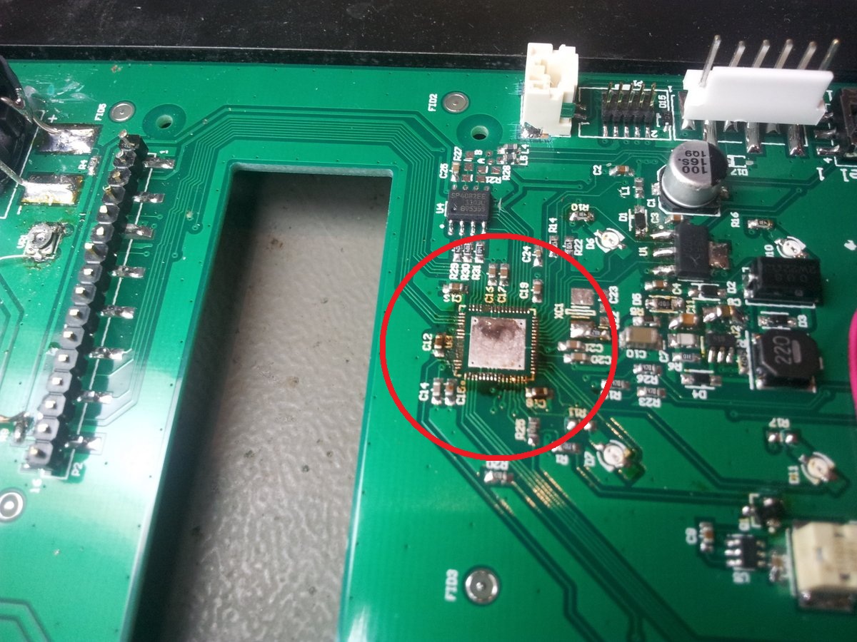
PCB Rework
Below is an example of a screwed PCB after too much rework was done on a 0.5mm pitch QFN package.
PCB Design Checklist
See the PCB Design Checklist.
Footnotes
-
STMicroelectronics. MB1136: NUCLEO-L073RZ Schematics. Retrieved 2022-09-23, from https://www.st.com/resource/en/schematic_pack/mb1136-default-c03_schematic.pdf. ↩