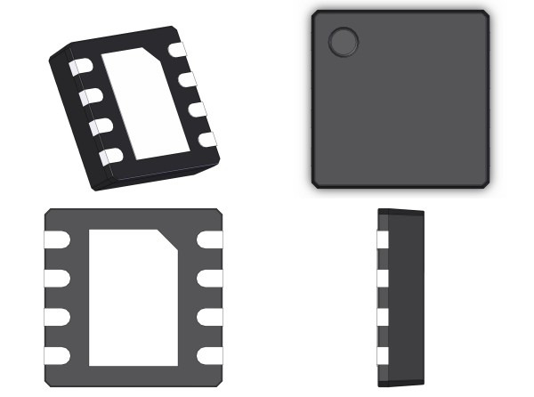
DFN Component Package

The DFN (Dual Flat No-lead) component package is also commonly known as the SON package. TI also calls this the Plastic Small Outline No-lead package.
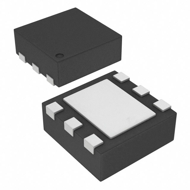
The DFN package is very closely related to the QFN package. From what I can tell, the main difference between the DFN and QFN package is that the DFN package generally only has pins running down two of it’s sides, while a QFN package has pins on all four sides. However, this is not a hard-and-fast rule, for example the V-DFN3020-13 (Type A) package by Diodes Inc. has pins on three of four sides1. The other big difference I have seen is that QFN packages seem to more standardized with consistent pin/package shapes and dimensions, whilst packages labelled “DFN” can have all sorts of “weird” pad/package geometries (see the below image).
JEDEC standard JESD75-5 specifies how generic logic circuits will be connected to certain pins of the DFN package.
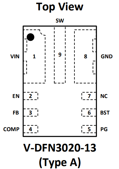
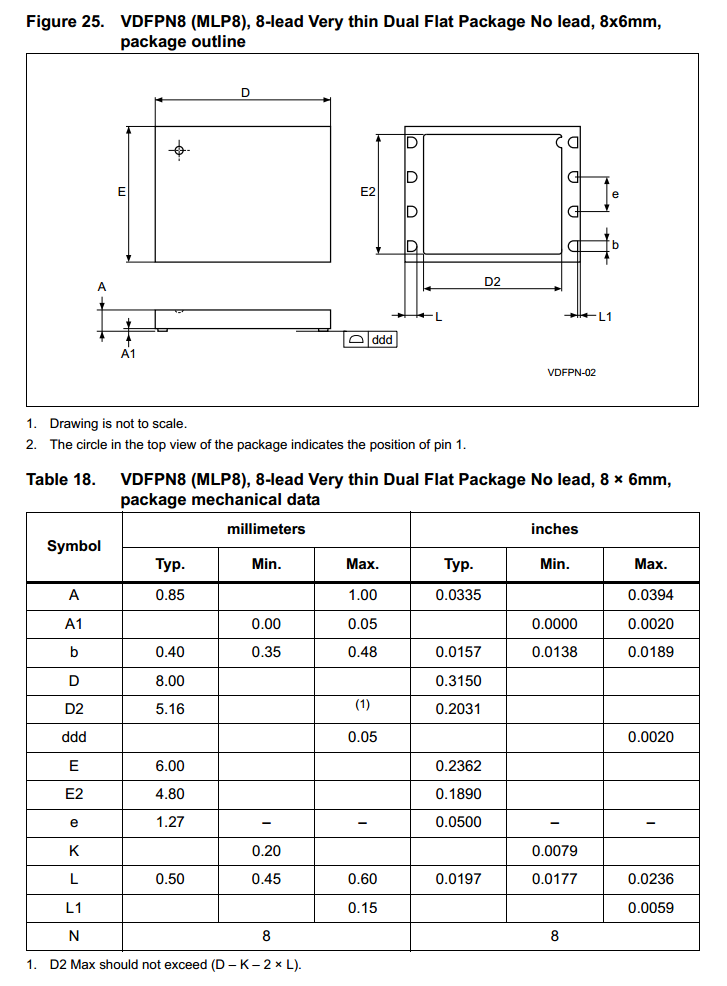
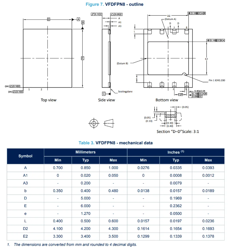
Below is an “odd shaped” SON package used by Numonyx flash chips that goes under the name VDFPN8. Notice the half-round appearance of the pins.
Texas Instruments AN-1187: Leadless Lead frame Package (LLP) is a great PCB designers reference document when using DFN or QFN packages (the document calls them LLP, but it is the same thing as DFN/QFN).
Synonyms
- DFN (Linear Technology, Micron Technology Inc, this synonym is more common than the JEDEC named SON!)
- DRC/S-PVSON-N9 (TI, DFN-10_1EP_3x3mm_P0.5mm_EP1.05x2.5mm)2
- DRP/S-PVSON-N6 (TI)
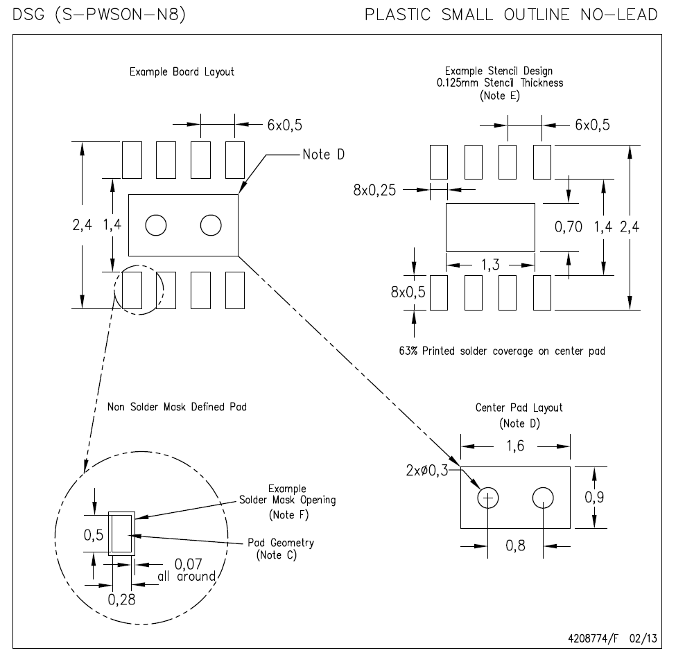
- DSG/S-PWSON-N8 (TI)
- LLP (Leadless Lead frame Package). The terminology used by National Semiconductor for their SON/DFN/QFN packages until they were acquired by Texas Instruments3.
- MFF2: Package name used for eSIM cards. Represents a DFN-8 package.4
- MLP (micro lead frame package or moulded leaded package). This also can refer to variants with pins on all four sides of the package, which is also called a QFN package. This name is used by Linear Technologies, Carsem.
- MLPD (MLP dual).
- MLPM (MLP micro). This name is used by Carsem.
- MLPQ (MLP quad).
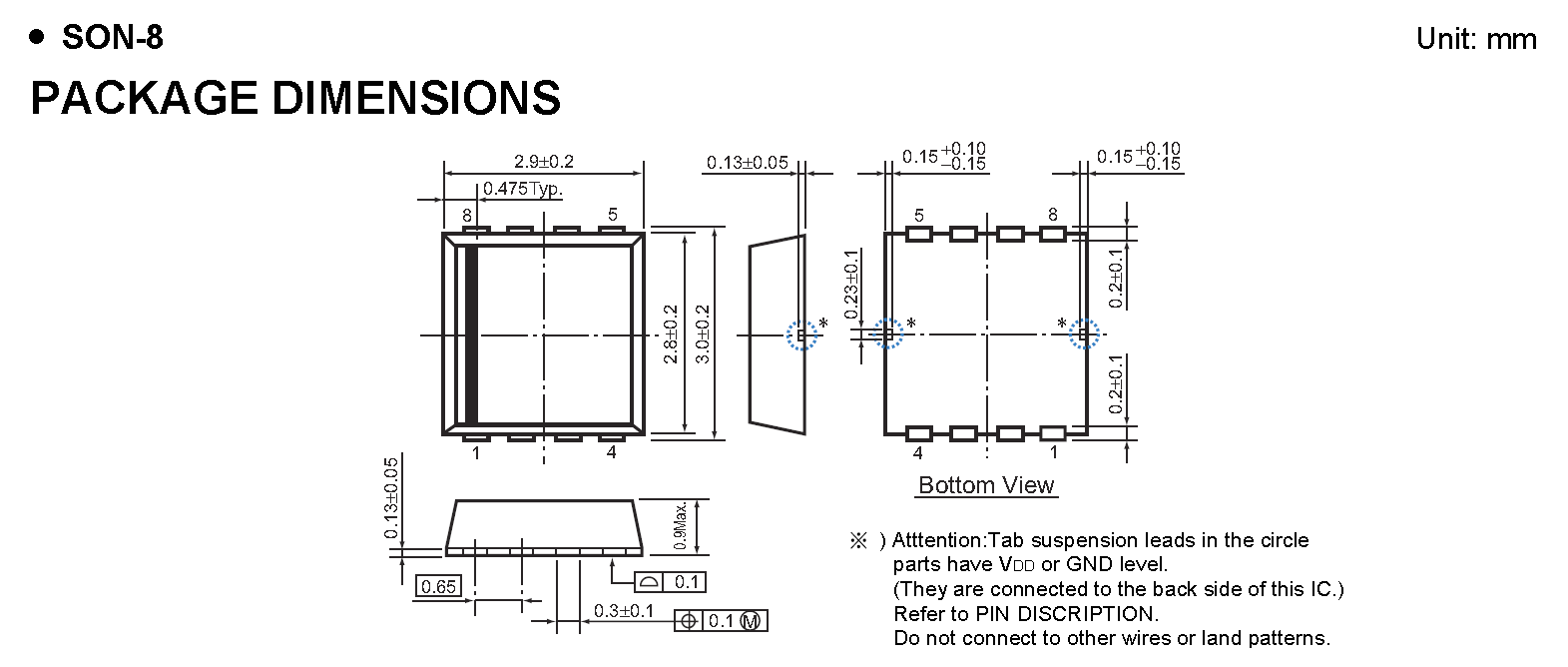
- PE-SON-8 (SON-8, Ricoh)
- SON (JEDEC)
- SW-PWSON-N8 (SON-8, TI)
- VDFPN (Numonyx, Micron Technology)
- VFDFN (DigiKey, e.g. part TPS54260DRCT).
- VSON (Texas Instruments)
- WDFN-6 (SON-6, On Semiconductor/Fairchild Semiconductor)
Variants
The SON package can have a varying number of pins. There are also VSON and WSON packages which are exactly the same as the SON package except for a different height. This package can also optionally include an exposed pad.
Similar To
- QFN (note that some may call SON a variant of QFN)
- SOD-882 (two pad package used for diodes)
- SOT-883 (three pad package used for transistors)
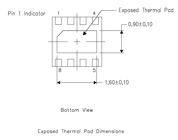
Thermal Pad
The SON package has a exposed thermal pad on the underside, similar to a QFN package.
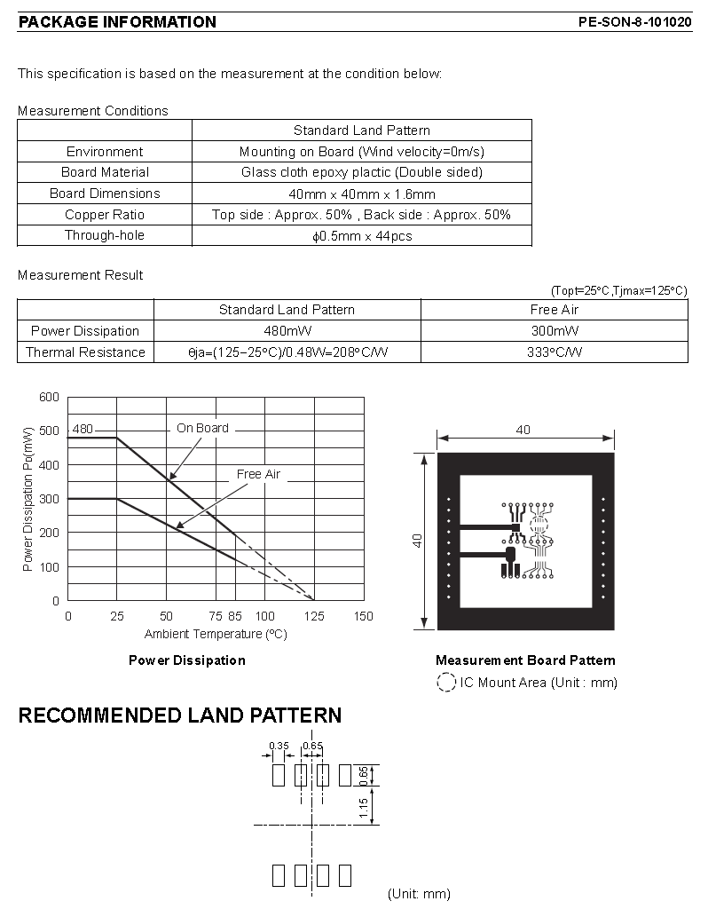
For a comparable TQFP package with the same pin count, the SON package (with an exposed pad) can usually handle more than twice the power dissipation.
Solderability
Reflow soldering is recommended. Hard to solder with a soldering iron due to underside thermal pad (some don’t have a thermal pad, and in that case, your chances are better). The tiny pitch is not so much of an issue as unlike the TQFP package, solder bridges are really easy to remove. You can solder the exposed pad in some cases by drilling a hole in the centre of the pad and soldering from the underside.
DFN-6, 3x3mm
The DFN-6 3x3mm package is used for components such as MOSFETs.
DFN-8, 3x3mm
The DFN-8 3x3mm package is used for components such as linear regulators5.
MFF2 (DFN-8)
MFF2 is a package that eSIM cards use. It is a DFN-8, that measures 5x6x1.27mm.6 The complete dimensions are shown in This is a placeholder for the reference: fig-mff2-dfn-8-package-dimensions-stm.
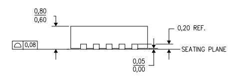
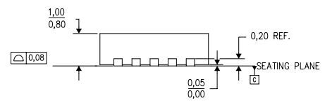
WSON And VSON Variants
The WSON and VSON variants of the SON package are identical to the SON package except for varying heights.
The WSON variant has a height of 0.80mm (max.)
The VSON variant has a height of 1.00mm (max.)
Common Uses
- MOSFETs
- Embedded SIM cards
- Solid-state load switches
- Flash memory ICs
Footnotes
-
Diodes Incorporated. 3.8V to 32V input, 3.5A low Iq Synchronous Buck with Enhanced EMI Reduction. Retrieved 2021-12-14, from https://www.diodes.com/assets/Datasheets/AP63356-AP63357.pdf. ↩ ↩2
-
Texas Instruments (2011, Sep). DRC (S-PVSON-N9): Mechanical Data. Retrieved 2022-10-06, from https://www.ti.com/lit/ml/mpss035d/mpss035d.pdf. ↩
-
Texas Instruments. QFN/SON package FAQs. Retrieved 2020-07-30, from https://www.ti.com/support-quality/faqs/qfn-son-faqs.html. ↩
-
STMicroelectronics (2021, Jan). ST4SIM-200M - eSIM GSMA system-on-chip solution for secure M2M industrial applications. Retrieved 2024-12-09, from https://www.st.com/resource/en/data_brief/st4sim-200m.pdf. ↩ ↩2
-
STMicroelectronics (2020, Apr). LDK715 (datasheet). Retrieved 2021-12-14, from https://www.st.com/resource/en/datasheet/ldk715.pdf. ↩
-
Velocity IoT. VIoT-Flex MFF2 - Multi-IMSI eUICC compliant eSIM card [datasheet]. Retrieved 2024-12-09, https://mm.digikey.com/Volume0/opasdata/d220001/medias/docus/4887/VIOT-1SIM-MFF2.pdf. ↩