HC-49/US Component Package

Published On:
Apr 4, 2015
Last Updated:
Apr 16, 2024
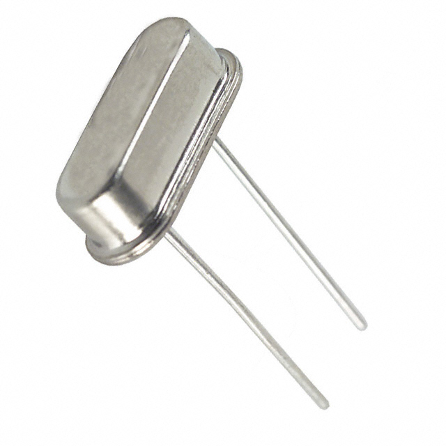
HC-49/US is a common component package for larger SMD crystals. The internal circuitry is shielded by metal case. It comes in 4 height variants (A, B, C and D). The power consumption of crystals in these package usually ranges from 1nW to 1mW, with a typical value being 50uW.
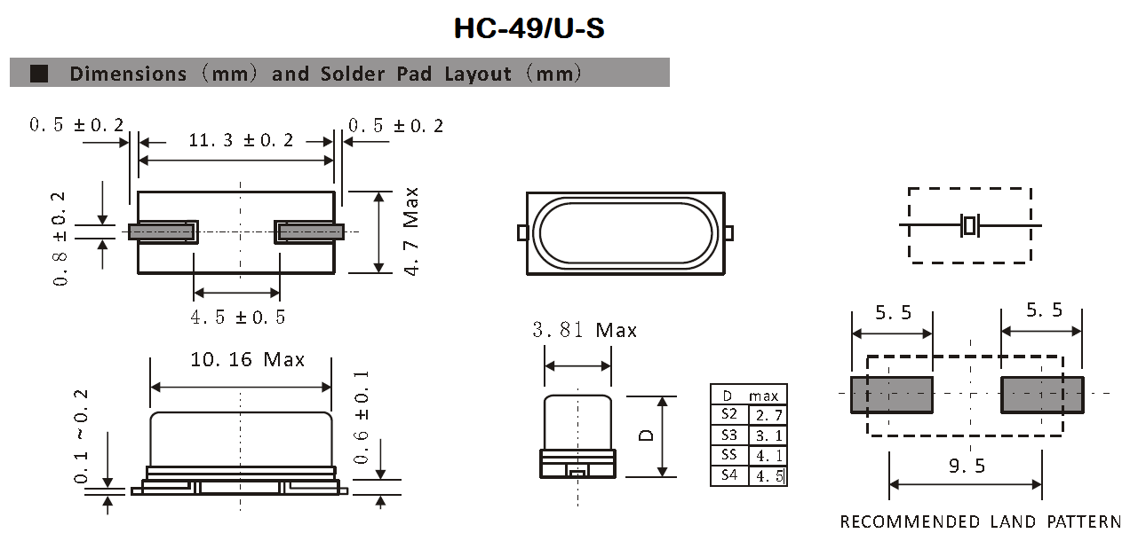
The pitch is 9.5mm. The package is easy to solder, as the leads extrude beyond the edge of the package. The PCB land area is 57.8mm2 (12.3x4.7mm).
Synonyms
- HC49/US
- HC-49US
- HC49-US
Variants
There a four variants for different height sizes (but same PCB land pattern). These are called A, B, C and D.
Similar To
- HC-49/S: Though-hole equivalent of the HC-49/US package.
Dimensions and Land Pattern
Further Reading
For info on un-named SMD crystal packages (which are more common than the HC-49/U-S due to their smaller size), see the SMD Crystal Packages page.