Testpoints
Test points are essentially a place on a PCB where you can connect a multimeter or scope probe and see what the circuit is doing (voltage wise). They are almost always necessary for prototyping PCBs and also for manufacturing if you ever want to diagnose faulty boards. Test points are becoming more important with the frequent use of SMD components since it harder to probe a component when they are fractions of millimeter wide. Back when through-hole components were in, every component was a test-point!
Current-based test points are harder to implement as you have to provide a way to break/rejoin a circuit (when using the traditional inline multimeter current measurement method). This is usually done with a jumper or cheap switch.
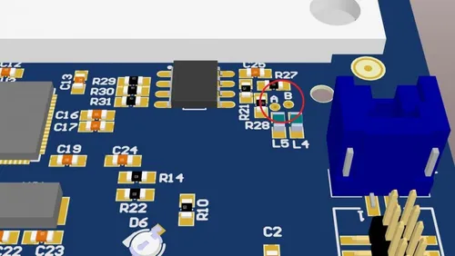
A common and easy way to add test points onto a PCB is to leave some vias untented. This means that they don’t get covered in solder mask, and you can easily probe them. Their circular nature holds the probe well to! The picture below shows two untented-vias, A and B, being used a test points.
Purpose-Built Testpoints
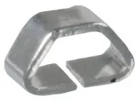
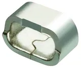
If you want a more serious testpoint something you can clip something onto, many manufacturers make custom testpoints. Even though these are designed to be miniature SMD test-points, the manufacturers normally recommend a largish land pad. Do not skimp on this, as you require this land-area so that the pad doesn’t rip of when you clip test leads to the test-point. Be warned, for what are seemingly simple pieces of bent metal, they are not cheap! Some examples are:
| Keystone Miniature SMT Test Point | Element14 Number: 385-8030 | |
| Harwin SMT Test Point | Element14 Number: 182-6282 |


