Altium Rules
Rules are used in the Altium PCB designer to both define the behaviour of certain PCB elements (such as the silkscreen expansion), as well as to set specific constraints for the PCB that will trigger a error when running the DRC (design rule checker). The latter is more important, and the rules in Altium are generally used to define things such as minimum track clearance, component clearance, and distance between silk screen and pads. Most of these rules are specified by the PCB manufacturer, otherwise general ‘rule of thumbs’ are used.
Access
Rules can be viewed, changed, and enabled by clicking Design -> Rules (as of Altium Designer Release 10). However, to make a design violation to show up in the DRC or as you a working on the board (an online DRC)
Unintuitive Problems
The Altium rules have some unintuitive problems which can cause plenty of grief when learning about how these rules are fully implemented.
Clearance Rules
Clearance rules on apply between objects on the same layer, no matter if you use the OnLayer('<layer name>') parameter, unless the rule is applied to the special Keep Out layer. This means that you cannot define a clearance between one object on one layer and another object on a different layer. This makes sense in most cases, but it also means you can’t define a board edge or other global ‘no go’ zones in anything but the Keep Out layer. A clearance rule applied between the Keep-Out layer and another object applies to all layers.
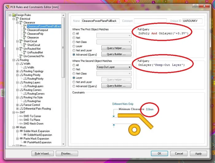
Power Plane Pull-back Rule
When designing a PCB, you have to make sure that all copper stays a certain distance away from the edges, as manufacturing tolerances result in a zone near the board edge which could potentially be cut through, resulting in broken tracks or exposed copper. This rule target’s polygon pours, and makes sure that they obey the clearance. The board outline has to be drawn on the keep-out layer for this to work. Make sure that the tracks on the keep-out layer are thin compared to the clearance required, otherwise the actual clearance distance will be significantly affected (Altium measures the clearance from the edge of the keep-out layer tracks, not the centre).
The following picture shows the rule in Altium.


