Oscillators

This site uses the word oscillator to represent a component with an self-contained oscillating feature that has power, ground, and signal out pins. This site uses the word crystal to represent an component which contains a oscillating element (in the form of a crystal), which requires an external oscillation circuit before it useful.
Designators
A common designator prefix to use for oscillators is (e.g. ). I do not recommend using the prefix as this should be reserved for crystal oscillators.
Important Parameters
Phase Noise
Phase noise is a way of describing the stability of the crystal in the frequency domain.
Start-Up Time
Symbol:
The start-up time for most oscillators is within the range 2-20ms. This start-up time can be important in low-power designs when the start/stop time of the crystal results in wasted energy.
MEMS Oscillators
MEMS oscillators are built using small mechanical structures (less than 0.1mm in any dimension) that vibrate at set frequencies when electrostatic forces are applied. This mechanical vibratory part of a MEMS oscillator is called the MEMS resonator. This is etched into a silicon die, and surrounding electronics contain both the driving, measuring, and compensation circuitry.
They use less power than a crystal-based oscillator, making them suitable for battery-powered devices. They are manufactured using standard IC manufacturing processes, so they are also more durable. They typically have better frequency stability over their operating temperature range, with common values being 10ppm at room temperature and 100pm over their entire operating temperature range.
MEMS oscillators do not like ultrasonic cleaning baths. Ultrasonic baths may permanently damage the oscillator or cause long term reliability issue1.
Packaging
MEMS oscillators have been made in packages which are also commonly used for crystal packages, such as the 2012 SMD package.
Some common industry sizes for oscillators include:
- 1612: 1.6 mm x 1.2 mm
- 2016: 2.0 mm x 1.6 mm
- 2520: 2.5 mm x 2.0 mm
- 3225: 3.2 mm x 2.5 mm
- 5032: 5.0 mm x 3.2 mm
- 7050: 7.0 mm x 5.0 mm
Wien Bridge Oscillator
The Wien bridge oscillator is a relatively simple oscillator that can generate reasonably accurate sine waves. It is named after a bridge circuit designed by Max Wien in 1891 for the measurement of impedances. William R. Hewlett (of Hewlett-Packard fame) designed the Wein bridge oscillator using the Wein bridge circuit and the differential amplifier.

However the modern way to draw this is to split up the non-inverting and inverting feedback circuits like this:

In my opinion this is a clearer way of drawing the circuit. Wien bridge oscillators are used in audio applications.
The series RC and parallel RC circuits form high-pass and low-pass circuit elements, respectively.
Wien Bridge Equations
Let’s first look at the series and parallel RC circuits that provide the positive feedback.
The impedance of the series RC circuit is:
The impedance of the parallel RC circuit is:
We can then write an equation for the voltage at the non-inverting pin of the op-amp in terms of the output voltage, and then describing it as a ratio we can get the gain of the RC network, (the symbol used here is consistent with the Barkhausen stability criterion):
Now if we focus on the purely resistive feedback network to the inverting pin of the op-amp, you should recognize this as the standard non-inverting gain configuration, where the gain is:
In steady-state oscillation, the reduction in amplitude of to as to be exactly “countered” by the gain provided from to . This is also known as the Barkhausen criterion:
Now lets aim to separate the real and imaginary terms and write it as an equation which equals 0:
For this equation to hold true, both the real and imaginary parts must be equal to 0. If we focus on the real part first we can find in terms of and :
Or in terms of natural frequency rather than angular frequency:
We can now look at the real part of the equation, which also must be 0. This gives us criterion for the ratio of the resistors and :
We can plug this back into the equation for the non-inverting gain of the amplifier so see what gain this results in:
Realistic Wien Bridge Oscillator Circuits
There is a problem with the above Wien Bridge oscillator circuits which limits them to the realm of theory only. It all comes back to the requirement that the Wien Bridge oscillator must have a loop gain of exactly 1 to function properly (Barkhausen stability criterion). If the gain is less than this, the oscillator will not start (or will stop if already started). If it is more than 1, the oscillator output will saturate and your sine wave output will start looking more like a square wave. Wien bridge oscillators typically need a non-linear component (a component which has a resistance which changes with applied voltage) to actively limit the loop gain and keep it at 1.
Common methods of actively limiting the gain include using:
- Incandescent bulb (resistance increases as it heats up)
- Diodes across in parallel with feedback resistors (resistance decreases as voltage increases)
- JFETs.
Wien bridge oscillators can also be made from a single supply2.
JFET Gain-Limited Example
Using a JFET to partially switch in another resistor in parallel with the ground-connected gain resistor in the Wien bridge oscillator circuit is another method for preventing the oscillator for saturating (as opposed to the diode method shown above). This JFET gain-limited approach is meant to introduce less distortion than the diode-limited approach above, as the RC circuit driving the JFET’s gate does not change much over a single cycle (assuming a suitable large RC time constant is picked).
Schematics of this technique are shown below, with the circuit setup to oscillate at the same frequency as the diode gain-limited variant mentioned above.
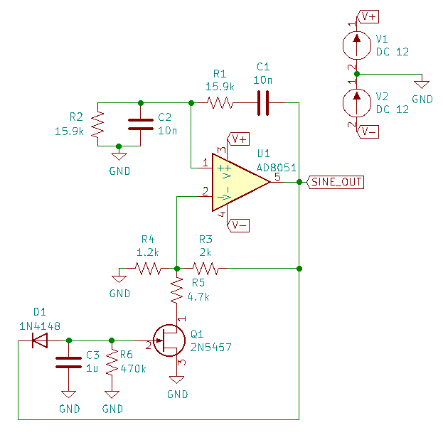
Note the diode and RC circuit controlling the JFET’s gate. When the circuit is first powered up, the gate is at ground and hence the gate-source voltage . Therefore the JFET is almost fully on (remember, JFETs are depletion mode devices), and is in parallel with , increasing the gain of the op-amp. As the output voltage beings to oscillate, on the negative part of the cycle, diode will conduct and charge the RC low-pass filter and with a negative voltage. This will decrease below , which will begin to turn the JFET off. This will then increase the equivalent resistance of in parallel with and decrease the op-amp gain. This will continue until the system reaches a steady-state and oscillates forever.
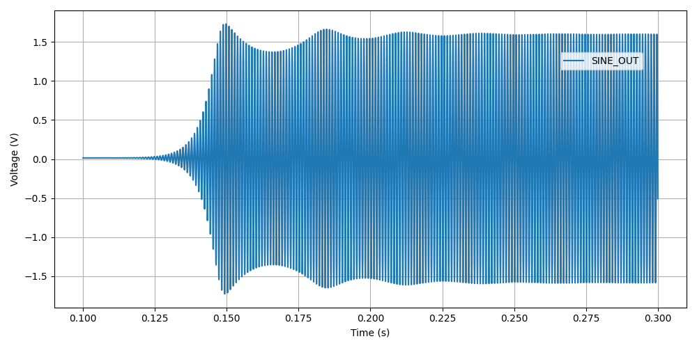
And below are the simulation results for this circuit:
Ring Oscillators
A ring oscillator (a.k.a. RO) is an electronic oscillator made up of a chain of an odd-number of digital logic NOT gates. The output of the last NOT gate is fed into the input of the first. The oscillator relies on the propagation delay from the input of the first NOT gate to the output of the last NOT gate to set the oscillation frequency.

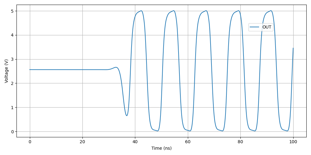
Simulation
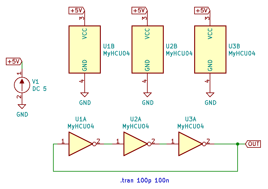
I ran into convergence issues when using the 74HCU04 SPICE model I found floating around on the internet (located in a file called 74HCng.lib). Simulating one instance of the inverter worked fine, but I got the dreaded doAnalyses: TRAN: Timestep too small error when connecting the second/third/e.t.c inverter in the ring. The convergence issue still occurred even when driving the first inverter instance from a slow frequency PULSE voltage source (rather than the driving it from the output of the last inverter), indicating it wasn’t a problem with the ring structure.
I then looked harder around the internet and found the MyHCU04 SPICE model posted on Google Groups by the late Jim Thompson:
On popular request, 74HCU04 Spice Model rescued from 1993 archives and posted on the Device Models & Subcircuits page of my website…
This SPICE model for an inverter fixed the convergence issues I was having (if anyone else is interested in this file, I’ve saved it here). Hurrah!
Manufacturer Part Numbers
- SiT1533AI: SiTime standard clock oscillators and MEMS oscillators.
- SiT1533AI-H4-D14-32.768G: MEMS clock oscillator.
Footnotes
-
https://www.mouser.com/datasheet/2/371/SiT1533_rev1.4_03202018-1324419.pdf, retrieved 2021-01-18. ↩
-
https://www.analog.com/media/en/technical-documentation/application-notes/AN-111.pdf, retrieved 2021-05-01. ↩