Junction-Gate Field-Effect Transistors (JFETs)

A junction-gate field-effect transistor (JFET) is a voltage controlled, three terminal transistor. It is closely related to the more popular MOSFET (another form of field-effect transistor).
The main differences between a MOSFET and a JFET is that the JFET has more gate current due to the absence of the gate oxide layer, and JFETs only come in depletion mode (JFET is on at , and turns off as goes negative), whilst MOSFETs come in both enhancement mode and depletion mode types.
Schematic Symbols
The below image shows the commonly used schematic symbols for JFETs. As with MOSFETs, there is an arrow pointing in towards the body for the N-channel, and an arrow pointing outwards for the P-channel.
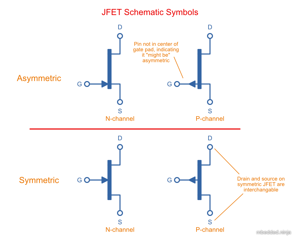
Interestingly, when you learn about the basic construction of a JFET, you would assume that the drain and source pins are interchangeable due to the symmetric nature of it’s design. That leads you to being able to use a schematic symbol with the gate pin in the middle of the gate. However, not all JFET pins are symmetric, and in that case it’s better to use the symbols shown which move the gate pin closer to the source (similar to how a MOSFET symbol is drawn).
Uses
JFETs are used for:
- Simple current sources
- Low noise op-amp input circuitry
- As a switch (although MOSFETs are more commonly used for this)
- Amplifiers
Datasheet Parameters
Gate-Source Cutoff Voltage ()
This is the gate-source voltage at which the JFET is pretty much “turned off”, i.e. the current flowing through the drain has dropped to almost 0. Typically it is specified as the voltage at which the drain current drops down to a current of . Unfortunately for JFETs, this value varies significantly due to manufacturing tolerances and typically a Vgs(off) min. to max. range of >5V can be given! Taking the OnSemi 2N5457 for example, it’s datasheet specifies a min. of and a max. of (ignore that because we are dealing with negative numbers, the max. is actually a “smaller” number than the min.)1.
Zero Gate Voltage Drain Current ()
This is the current through the drain when .
Gate-Source Breakdown Voltage ()
The gate-source breakdown voltage is the maximum voltage the gate can withstand (relative to the source) before breakdown occurs.
Transconductance ( or )
The transconductance (also called small-signal transconductance, forward transfer admittance , or ) is the ratio of change in to a change in at a constant drain-to-source voltage (see the below equation). It is typically given in units of (or , which is equivalent). It can be thought of as the small-signal gain, when the JFET is operating at a fixed DC bias point.
The transconductance is maximum at , which is called and is typically specified in the JFET’s datasheet2. The below image shows the curve of vs. for the 2N5457 JFET.
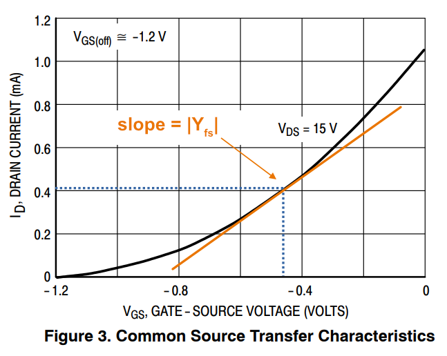
The transconductance for most JFETs ranges from . They are typically specified at the bias point
Output Conductance
The output conductance is the ratio of change in to a change in 3.
ranges from to for most JFETs3.
The output conductance is an important consideration for the stability/accuracy of a JFET current source3. Another way of expressing output conductance is the [^#_dynamic_resistance, dynamic resistance].
Dynamic Resistance
The dynamic resistance is just the reciprocal of the [^#_output_conductance, output conductance], and is typically expressed in units of .
Current Source
JFETs can be used to make two-terminal current sources which can be useful in circuit design due to their simplicity. See Current Sources And Sinks: Constant-Current Diode (JFET Current Source) for schematics, how they work, and equations for calculating the values. They can also be used to make low-noise current sources.
Common Components
- 2N5457: Common “general purpose” N-channel JFET.
- J202: N-channel JFET by ON Semiconductor that originally came in a TO-92 package, but now comes in a SOT-23-3 package.
Parameters for popular JFET parts:
| Part Number | Package | |
|---|---|---|
| 2N54571 | TO-92 |
Footnotes
-
On Semiconductor (now On Semi) (2010, Feb). 2N5457, 2N5458 JFETs: General Purpose N−Channel − Depletion (datasheet). Retrieved 2022-01-11, from https://www.onsemi.com/pdf/datasheet/2n5457-d.pdf. ↩ ↩2 ↩3
-
Electrical 4 U (2020, Oct 28). Parameters of JFET or Specifications of JFET. Retrieved 2022-01-13, from https://www.electrical4u.com/parameters-of-jfet-or-specifications-of-jfet/. ↩
-
Siliconix (now Vishay) (1997, Mar 10). AN103: The FET Constant-Current Source/Limiter. Retrieved 2022-01-13, from https://www.vishay.com/docs/70596/70596.pdf. ↩ ↩2 ↩3