PCI Express (PCIe)
PCI Express (PCIe) is a high-speed serial bus, designed as a replacement for the older parallel PCI or PCI-X buses.
PCIe is a packet based network, similar to Ethernet. However, it is accessed via reads and writes to/from the address and I/O space, and there are vendor and product IDs, so in a large way it mimics the older PCI bus.
Child Pages
Layers
The PCIe specification defines three networking layers, the transaction layer (the topmost layer), the data link layer, and the physical layer (the bottom layer).
The Transaction Layer
The transaction layer is where transaction layer packets (TLPs) are defined. This is the uppermost layer of the PCIe specification.
There is a restriction of the maximum number of bytes per TLP. Typical maximums are 128, 256 or 512 bytes. Larger bits of information have to be split over multiple TLPs.
The Data Link Layer
The data link layer is responsible for making sure that every TLP (transaction layer packet, see above) arrives at it’s destination correctly.
It gets the TLP and wraps it with it’s own header and CRC. It also implements a acknowledge-retransmit protocol so that no TLPs are lost during transmission. Flow control is also implemented in this layer, to make sure that the receiver is ready to receive the packet before transmitting it.
The data link layer also implements the data-encoding scheme. PCIe v1.x and v2.x use the 8b/10b encoding scheme, while PCIe v3.0 commonly used 64b/66b encoding.
The data link layer can also do packet re-ordering.
Lanes
Each lane consists of two uni-directional differential LVDS or PCML pairs. Therefore each lane requires 4 signal traces, excluding power and ground.
Up to 32-lanes are supported with a single PCIe.
The minimum implementation of PCIe with one lane requires 4 wires for data transmission and 2 for a reference clock, giving a total of 6 (excluding power and ground).
| PCIe Version | Transfer Speed |
|---|---|
| v1.x | 2.5GT/s |
| v2.x | 5.0GT/s |
| v3.0 | 8.0GT/s |
| v4.0 | 16.0GT/s |
Links
A link is a device-to-device connection consisting of 1 or more lanes.
One of the cheapest FPGAs with PCIe support is the XC7A35T-1FTG256C, a Xilinx Artix-7 with 33280 cells in a BGA-256 package. In Feb 2015, it was available from Avnet Express is prices of US29.17 (500).
Data Transmission
Data is transmitted in big-endian format (as per PCI Express Base Specification).
Memory
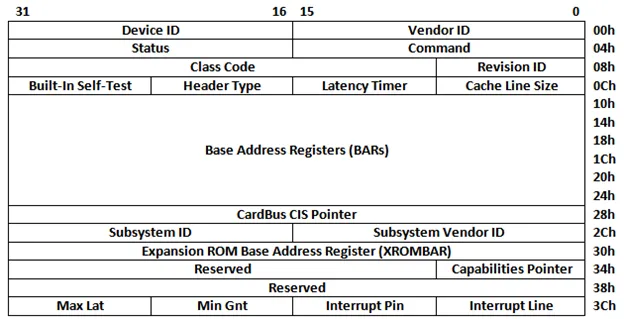
PCI devices have a set of registers referred to as the configuration space, and PCIe introduced the additional extended configuration space. These spaces are memory mapped so that device driver software can access them.
Configuration Space
The configuration space is a standardized section of memory on PCIe cards that allows PCIe cards to configure correctly.

What Are BARs?
Base Address Registers (BARs) are the starting addresses of a contiguous mapped section of system or I/O memory.
The endpoint requests a block of memory.
Bridges
Because of how PCIe was designed, it is possible to build bridges between PCI and PCIe without any loss of functionality. This can be done without any change in software (i.e. the software still thinks it is talking to a PCI bus).
PCI Express to generic local bus bridges. One example is the PEX8311 made by Avago.
There is also a PCI Mini Express Card size. They are not physically compatible with full-size PCIe slots, but there are passive adapters to convert between the two sizes.
Testing PCIe Carts With A Computer
Once you have designed and made a PCIe card for a computer, one of the first things you’ll want to do is plug it into a PCIe slot on the computer as see if the computer recognizes it.
The way to detect and explore the PCIe device depends on the OS that the computer is running.
Windows
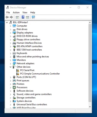
The built-in Device Manager gives a very brief overview of detected PCI cards.
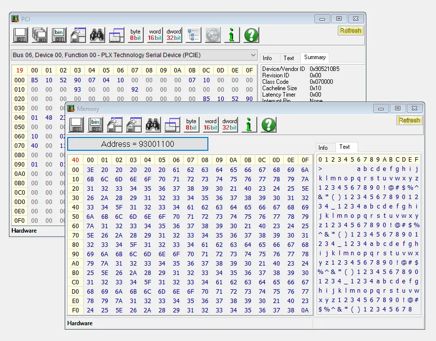
RWEverything is a great Windows tool that allows you to read and write from any available memory location on the PCIe card (not just the configuration memory, as many other tools provide).

Manufacturers
PLX Technologies is now Avago Technologies.


