MOSFETs
A MOSFET (big breath now…it stands for…Metal-Oxide-Semiconductor Field-Effect-Transformer) is a three-pin active semi-conductor device, used frequently in electronics design. In the most basic sense, they can be thought of as a voltage controlled switch that can turn things on and off (or partially on, when used as an amplifier!).
MOSFETs should not be confused with similar but different semiconductor devices such as MODFETs (modulation-doped FETs) or MESFETs (metal-semiconductor FETs). Depletion-mode MOSFETs are closely related to JFETs.
Uses
- Basic electric switches (turn a load on/off)
- Totem-pole drivers
- H-bridges
- 3-Phase Inverters
- Current regulating shunts (with feedback)
- Switch-mode PSUs
Types And Schematic Symbols
Enhancement-Mode
Unfortunately for the keen circuit designer learning about MOSFETs, there is a dizzying variety of MOSFET symbols in use, owing to the fact that there are a larger number of different MOSFET types, and that no one can agree on a single standard. This section will walk you through all the various types. The below image shows the commonly used schematic symbols for enhancement-mode MOSFETs, with both the N-channel and P-channel variant.
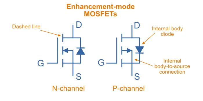
The arrow in the symbol has it’s origins from a simple diode, in which the arrow points from the P-type substrate to the N-type substrate (which is also the direction of conventional current flow through a diode). Sometimes an outer circle is added to the above symbols, since a MOSFET is a transistor and by convention transistors are drawn with circles (e.g. think about a BJT symbol). However this has been omitted from the above symbols as it does contribute somewhat to the “noisyness”, I find the circle-less symbol much cleaner. Totally a personal preference though.
Depletion-Mode
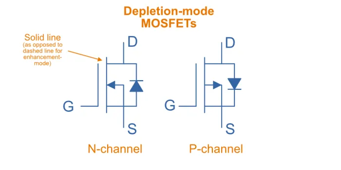
Although not as popular as enhancement-mode MOSFETs, depletion-mode MOSFETs are a very important MOSFET type. They are typically distinguished on schematics from enhancement-mode types by drawing a solid line rather than a dashed line for the channel, as shown below:
The easiest way to show the difference between enhancement and depletion-mode MOSFETs is to plot a vs. graph as shown below:
The curve for the depletion-mode MOSFET is shown on the left. As you can see, the device is OFF (not conducting current) when is around and is well and truly on when gets to . In comparison, the enhancement-mode MOSFET is fully off when , and takes around before it starts conducting.
Depletion-mode MOSFETs are used for:
- Bi-directional current limiting circuits (which can also withstand high voltages)
- Current sinks/sources
- Attaching onto the input of a linear regulator to allow it to run of high voltages (or protect it from ESD)1.
Alternate Style #1: Arrows
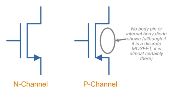
Sometimes the body connection, body diode and enhancement/depletion mode indicators are removed altogether from the schematic symbol, and a simplified set of symbols is used as shown below:
Alternate Style #2: Polarity Dot
The difference between N-channel and P-channel MOSFETs may be instead distinguished by adding a inverting-style circle on the gate pin as shown below. This symbolises that a P-channel is the inverse of the more typical/standard N-channel (in a sense).
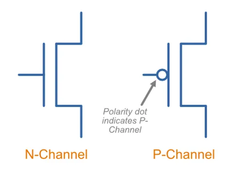
This style is commonly used when drawing MOSFETs as part of logic gates and other integrated circuitry, due to it’s simple and small symbol size which does not clutter the page when illustrating complex logic that might use 10’s or 100’s of these devices. Also, due to the substrates being connected to the rail voltage and ground, the drain/source are symmetric and there is no need to distinguish between the two.
CMOS 4-pin MOSFETS
MOSFETs inside ICs do not normally have the substrate connected to the source, an are instead drawn as four pin devices, of which the additional fourth pin is connected to the substrate (a.k.a. four-port MOSFETs). When using CMOS technology, N-channel MOSFETs are typically connected to the negative voltage rail (e.g. ), and P-channel MOSFETs connected to the positive voltage rail (e.g. ). Note also that as soon as you disconnect the substrate from the source, the drain and source pins no longer have any differences, i.e. they can be interchanged and the device will still work as expected. Also, because the source-to-substrate is not shorted out, the MOSFET now has two internal back-to-back diodes, rather than just the one, and can block current in both directions.
ICs such as voltage-level translators and analogue switches use this substrate connection to their advantage (especially the part about blocking current in both directions).
For more information on this, see the The Body Effect And Connecting The Substrate To The Source section below.
Important Parameters
Note that with all voltage parameters that mention two pins of a MOSFET (e.g. ), the voltage is measured from the first pin to the second pin (e.g. from the drain to the source). This would be the same as connecting the red probe of a multimeter to the drain, and the black probe to the source.
Sorted by alphabetical order, including subscripts.
Rds(on)
is the on-state drain-source resistance. The resistance between drain and source when the MOSFET is turned on with a strong gate drive and low (hence in the linear, Ohmic region of operation). Usually around for smaller MOSFETs, and can be as low as for larger power MOSFETs. is roughly linear with the maximum drain-source voltage of the MOSFET. For this reason BJTs or IGBTs (which both have a BJT like output) are instead preferred for high-voltage high-current applications, when the voltage starts to exceed 400V.
Vds(max)
is the maximum drain-source voltage. It is the maximum allowed voltage between the drain and source. A higher voltage can cause the MOSFET to breakdown. This is commonly just called the voltage rating of the MOSFET, as it describes the maximum voltage it can withstand between it’s “switching” terminals.
Vgs(max)
is the absolute maximum gate-source voltage (aka gate-source breakdown voltage). Voltages above this may irreversibly destroy the MOSFET. This is due to the very thin gate-oxide layer (100nm thick, or less!) that separates the gate from the MOSFET channel, which is easily destroyed by a “high” voltage. This can be called oxide breakdown. is very commonly for a huge variety of MOSFET families.
Because of the very high impedance of the gate pin, MOSFET devices are very sensitive to static electricity. Especially so when not soldered into any circuitry. It does not take much charge on the gate to exceed the max. gate-source voltage and destroy the MOSFET. Anti-static precautions are recommended when handling individual MOSFETs (i.e. anti-static mats, discharge wrist straps).
Vgs(th)
is the gate-source threshold voltage (or just threshold voltage). The voltage between the gate-source at which the MOSFET begins to turn on. The point at which it “begins to turn on” is defined by the manufacturer and should be mentioned in the datasheet. Typically is is a certain drain current, e.g. .
How To Use Them?
The amount of current through the drain-source in controlled by a voltage on the gate. To make a basic switch, you can insert an N-Channel MOSFET between the load and ground. The source is connected to ground, and the drain to the negative terminal of the load. If the gate is given 0V (aka connected to ground), the switch will be off. If significantly more than is applied to the gate, the MOSFET will fully turn on (conduct current), and the load will get power.
P-channels work in a similar manner to N-channels, the difference being that a negative has to be applied to turn them off (that is, the voltage on the gate has to be less than that on the source). This results in them commonly being used for high-side switching, in where the source is connected to , the drain to the load, and the gate voltage pulled low to turn it on, or pulled-up to to turn it off.
In any case, do not leave the MOSFET gate floating. Since it has a very high impedance input, if the gate is not driven, then noise can change the voltage on the gate, and cause the MOSFET to conduct/have undefined behaviour.
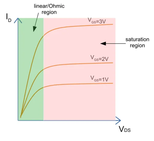
The above examples describing switching a MOSFET from it’s fully off state to it’s fully on state. But if you apply a at or just above , the MOSFET will only partially turn on. The below image illustrates a MOSFETs behaviour:
Leakage Current
Leakage current is an important parameter to consider when you are using the MOSFET for switching on-and-off other circuitry in a low power design. MOSFET have both a gate-to-source and a drain-to-source leakage current. Typically the drain-to-source leakage current is 10x greater than the gate-to-source leakage current. The drain-to-source leakage current increases greatly with an increase in temperature. Typical values at 25°C are for the gate-to-source leakage current and for the drain-to-source leakage current.
If you need lower leakage currents that what you can achieve with a MOSFET, try using a J-FET. They have typical leakage currents of .
Failure Modes
There are three ways in which a MOSFET can generally fail:
- Gate punch-through: Occurs when a large voltage spike appears on the gate that exceeds the maximum gate-source voltage (typically 10-20V). It punches a hole in the weak oxide layer.
- The drain-source voltage exceeds the rated maximum
- Overheating
To prevent over-voltage failure’s, TVS diodes, Zener diodes, or snubber circuits can be used to protect the pins. TVS and Zener diodes are the most common ways to do this, and are used to clamp the voltages to a safe level.
Almost always, a MOSFET will short out the drain and source when it fails. This mean the MOSFET goes into conduction, and can destroy even more circuitry! Either make sure that your MOSFET won’t fail, or take precautions against large currents if it does. I experienced plenty of MOSFET failures when designing the half-bridge for the Electric Skateboard project.
Thermal Stability
The drain-source resistance of a MOSFET increases with an increase in temperature (a BJT behaves in the opposite manner, it’s collector-emitter resistance decreases with an increase in temperature).
This means that MOSFETs can share current with each other easily. The positive temperature-to-resistance coefficient creates a self-balancing current mechanism for MOSFETs connected in parallel. Just make sure each MOSFET has its own gate drive resistor! Directly connected MOSFET gates can cause weird oscillation problems.
Dead-Time
Dead-time is a technique which is commonly applied to MOSFET driving when the MOSFETs are in a H-Bridge (or half-bridge) configuration. Dead-time is the time between when one MOSFET(s) is turned off and another MOSFET(s) is turned on. It is used to prevent shoot-through, which is when two MOSFETs on the same leg of a H-bridge are on at the same time, creating a direct short between and . Shoot-through occurs because of the turn-off delay time of a MOSFET.
Turn On/Turn Off Times
In precise pulse-drive situations, it is desirable for the MOSFET to have similar turn-on and turn-off times. This is so the output pulse, although delayed by these parameters, has roughly the same width as the input pulse to the gate. This is important in applications such as laser range-finding.
Different MOSFET Construction Methods And Industry Names
Sorted alphabetically by name.
DMOS FET (Double-Diffused MOSFETs)
The DMOS (Double-Diffused MOSFET) was first developed in 19692.
FinFETs
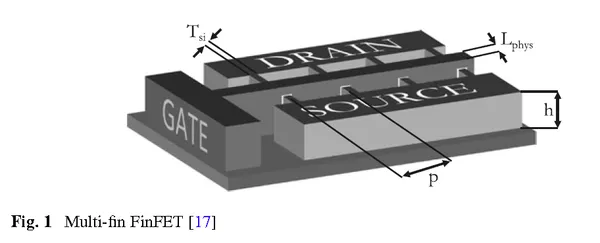
FinFETs are multi-fin FETs which overcome issues once MOSFET approach very small sizes (such as 22nm).
FRFET
A trademarked name by Fairchild used to label some of their fast-recovery MOSFETs used in inverter and BLDC controller design
HEMT
The high-electron-mobility transistor (HEMT) is not technically as MOSFET, but is very closely related. It is a field-effect transistor which contains a junction between two materials with different band gaps3.
LDMOS (Laterally-Diffused MOSFETs)
PROFET
A name (it stands for protected-FET) used by Siemens and now Infineon to describe power MOSFETs with built in logic circuitry for “smart switches”, designed for controlling current and voltage into a load. An document about PROFETs from Infineon can be found here.
Trench MOSFETs
Trench MOSFETs give a very low per unit silicon area.
Gallium Nitride (GaN) MOSFETs
Gallium Nitride (GaN) MOSFETs switch much faster than traditional silicon MOSFETs4, resulting in lower switch losses in power electronics and higher-frequency operation. This is because they have much smaller gate-to-drain capacitance than their silicon counterpart5.
One example of a GaN MOSFET is Texas Instrument’s LMG3525R030-Q1. It is a GaN MOSFET with an integrated driver, protection and error reporting. The driver supports switching speeds of up to 150V/ns6.
MOSFET Applications
Load Switching
MOSFETs can be used for load switches, as shown on the Load Switches page. They can be used in a back-to-back configuration for creating AC solid-state relays (SSRs).
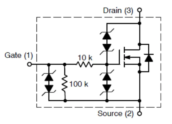
Some MOSFETs designed for switching loads support logic-level inputs (e.g. +3.3V or +5.0V from either a microcontroller or logic gate) and have built in TVS diodes. One such example is the DMN61D8L-7 from Diodes Incorporated. As shown below, this particular MOSFET package also included a pull-down resistor and ESD limiting resistor in series with the gate.
Isolated Gate Drives
One problem with MOSFETS (well, with any switched semiconductor) is dealing with the gate drive when either:
- A) The source voltage is not constant or at a point where the gate-source voltage for turn-on is not easy to achieve
- B) The MOSFET is dealing with large voltages and so electrical isolation between the load and the drive circuitry is desired/required (normally by law)
In these cases, the gate drive has to be isolated.
IRF - Application Note AN-937 - Gate Drive Characteristics And Requirements for HEXFET Power MOSFETs is a great article on isolated gate drive techniques.
Amplifiers
Common-Source Enhancement-mode MOSFET Amplifier
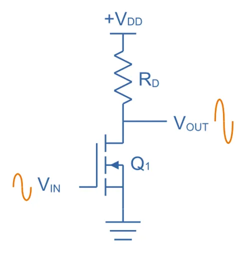
A common-source enhancement-mode MOSFET amplifier is a basic MOSFET-based amplifier. The most popular variant is based of an N-channel enhancement-mode MOSFET (although you can make common-source amplifiers with P-channels too!), in which the source is grounded. It is called a “common-source” amplifier because the source is a shared (common) terminal between the input and output. It is closely related to the BJT common-emitter amplifier. Like the common-emitter amplifier, it is an inverting amplifier.
The huge problem with the above circuit is the non-linearity.
Bi-directional Current Limiter
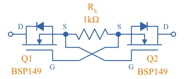
An interesting use for depletion-mode MOSFETs is a simple bi-directional current limiter circuit. The below image shows the schematic, which uses two depletion-mode MOSFETs connected back-to-back with a resistor in-between.
The circuit above utilizes the depletion-mode MOSFETs unique feature of being on when the gate-source voltage is 0V. The circuit works like this:
- When no current is flowing, no voltage is dropped across the resistor. Hence both MOSFETs is 0V. Because these are depletion-mode MOSFETs, this means they are turned on, and the circuit appears as a resistance of value .
- As current begins to flow from left-to-right, a voltage drop begins to appear across . This creates a negative for and a positive for . We can ignore the positive as this only serves to turn a little more (note that even if wasn’t on, it’s internal body diode would conduct anyway). However the negative on is important!
- As the current reaches a certain value, across will become negative enough to reach it’s (which is between -2.1V and -1V for the BSP1498). At this point it will begin turning off, will begin to drop voltage across it and hence limit the current of the circuit.
- Because of the symmetry this circuit works in exactly the same way if current is flowing in the other direction (right-to-left), but with the roles of and reversed.
Worked Example of the Bi-directional Current Limiter
The figure above shows two BSP149 MOSFETs and an .
From the datasheet of the BSP149, is between -2.1V and -1V8. Unfortunately is never a well defined parameter, so we’ll just pick a value in the middle of .
This means that the circuit should limit the current to approximately:
Because you can get depletion-mode MOSFETs with a maximum rating of 200-1000V, this circuit is an excellent candidate for protecting the input of something that could expect either a high positive or negative voltage.
TIP: Because of the part-to-part uncertainty in , this circuit is suitable for crude current-limiting (e.g. for circuit protection) but not for designing an accurate current sink/source.
Internal Diodes
Because any PN junction is inherently a diode, a regular MOSFET has two of them. One of the diodes is removed when the substrate is connected to the source, which is usually done for any 3-pin discrete MOSFET component.
The Internal BJT
Aside from the two naturally occurring diodes, MOSFETs also contain a BJT. The source-substrate-drain layers form either an NPN or PNP BJT. You don’t normally have to worry about this “parasitic” element.
CMOS devices have PNPN structures. This forms a parasitic thyristor, which can cause latch-up.
The Body Effect And Connecting The Substrate To The Source
The basic design of a MOSFET provides four (not three!) electrical connection points. However most discrete MOSFET components only provide 3 leads from the package. This is because the substrate (body) lead is normally connected internally to the source, so you only get three external connections (Gate, Source/Substrate, and Drain). The below image shows the internal silicon structure of a MOSFET.
Some discrete MOSFETs do provide you with a separate substrate pin, for example the 3N163 as shown below:
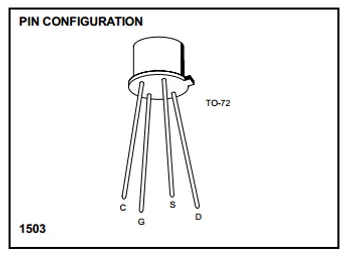
The body effect (also known as the Substrate Bias Effect) of a MOSFET describes how the threshold voltage of a MOSFET, is affected by the voltage difference between the substrate and source, . Because the source-to-body voltage can effect the threshold voltage, it can be thought of as a second gate, and the substrate sometimes called the back gate, and this effect called the back-gate effect. For a N-channel MOSFET, as the substrate becomes more negative than the source, the threshold voltage of the MOSFET is increased.
Note that most discrete MOSFETs that you can buy internally tie the substrate to the source, meaning . This prevents any body effect from occurring.
For a N-channel MOSFET, the threshold voltage is affected by the body effect as governed by the following equation9:
where:
is the threshold voltage with substrate bias present [Volts]
is the threshold voltage for zero substrate bias [Volts]
is the body effect parameter
is the source to body (substrate) voltage [Volts]
is substrate Fermi potential
The body effect parameter is:
Another interesting note is that without the connection of the substrate to the source, the MOSFET source and drain connections would be identical, and there would be no need to separately identify them. As soon as the substrate is connected to the source, the MOSFETs internals become asymmetrical and you cannot freely swap around the drain and the source (if you do swap them, you’ll normally get the body diode conducting when you don’t want it to!).
For a N-channel MOSFET, when the substrate is not connected to the source, whatever N-doped implant is most negative in voltage will be the source. The important gate-source voltage to turn the MOSFET on will then be measured between the gate and this implant.
Why is the substrate normally connected to the source?
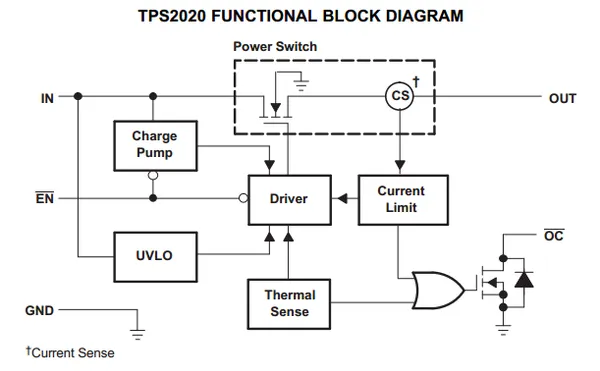
The substrate is normally connected to the source in most discrete MOSFETs because it makes the MOSFET easier to use. If the substrate is not connected to the source, you have to consider the body effect. It is easier/better to connect the substrate to the source internally (less connection resistance, one less lead, e.t.c) rather than to leave it up to the circuit designed to connect it externally. Manufacturers of ICs with integrated MOSFETs may choose to connect the substrate to something else. A common choice is ground.
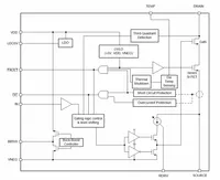
When doing IC design, the substrate is often NOT connected to the source. The TPS2020 load switch by Texas Instruments is one example. You can see below that the substrate pin of the MOSFET at the top of the image is connected to ground.
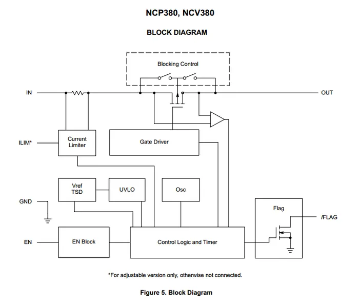
Another example is the NCP380 high-side load switch by On Semiconductor. Notice how in the below image the substrate of the MOSFET is connected to two switches, which can either connect it to the input or the output.
The Transconductance Of A MOSFET
The transconductance of a MOSFET is the ratio of a change in output current (drain-source current, ) due to the change in input voltage (gate-source voltage, ) over an arbitrarily small range of operation.
The range of operation has to be restricted because the transconductance of a MOSFET changes depending on the operating point.
Spice Model
Information about the MOSFET Spice model can be found on the Altium Simulation page.
Floating-gate MOSFETs
A floating-gate MOSFET (FGMOS) is a type of MOSFET where the gate is completely isolated. Isolation in this sense refers to no connection via conductive materials such as copper or doped semiconductor. The gate is capacitively coupled to one or more “input gates”. Because the gate is isolated (the gate can also be thought of as “floating”), any charge stored on it via the capacitive coupling remains there for a long time. This forms the basis of a floating-gate memory cell which is used to provide the storage in non-volatile memory such as EEPROM and flash. The cell “remembers” the state it was last in, for long periods of time, even when power is removed from the circuit.
How long will floating-gate MOSFETs retain their charge, if un-powered? As of 2020, the current mass-produced, consumer grade flash memory devices and SD cards claim to have a memory retention life of approximately 10 years, if left un-powered the entire time (if periodically plugged in, these devices can re-charge and “reset” the 10-year clock).
Split-Gate MOSFETs
A very critical parameter for a MOSFET is it’s on state resistance. The easiest way to reduce this is to increase the doping concentration of the epitaxial layer10. However this also decreases the breakdown voltage. The Split Gate MOSFET structure is a design that has been developed to allow the on resistance to decrease whilst keeping a high breakdown voltage. Comparing a standard MOSFET with a split-gate MOSFET to which both have the same breakdown voltage, the on resistance of the split-gate MOSFET can be around 50% lower.
Current Sensing MOSFETs
The IXTN660N04T4 by IXYS is one example of a current-sensing MOSFET.
On Semiconductors application note AND8093/D has some great reading material on current sensing MOSFETs.
Manufacturer Part Number Families
- 2N7002: N-channel, 60V, 300mA MOSFET from a variety of manufacturers.
Part Recommendations
Link to DigiKey’s (US) MOSFET selection (single/discrete): https://www.digikey.com/en/products/filter/transistors-fets-mosfets-single/278
PMV45EN - N-Ch
- Manufacturer: NXP
- Manufacturer Part Number: PMV45EN
- Supplier: Element 14
- Supplier Part Number: 108-1483
- Supplier Price: NZ0.25 (100)
The PMV45EN is a low cost, very low RDS(on) N-Channel MOSFET which I use as the work horse for most of my projects. It has an RDS(on) of only 35mOhm and is rated for a current of 5.4A. The maximum drain source voltage is 30V, making it suitable for most embedded, low voltage applications. Also in the PMV range is the PMV90ENER.
DMN3731U - N-Ch
- Manufacturer: Diodes Incorporated
- Manufacturer Part Number: DMN3731U (datasheet)
- Package: SOT-23-3
- Suppliers:
With an max. of when , this N-channel MOSFET can be directly connected to GPIO lines on a +3.3V MCU.
MOSFET Safe Operating Areas
The section is in notes format and needs tidying up.
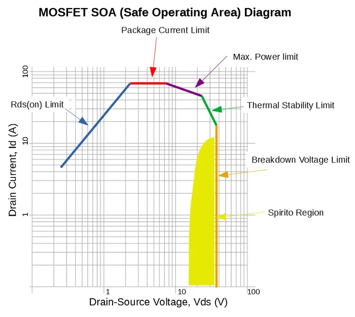
A MOSFET’s SOA (Safe Operating Area) is usually shown as a graph in the datasheet. The SOA graph shows which combinations of drain-source voltages and drain currents are safe and which will likely damage the MOSFET. The graph takes into account steady-state operating conditions (i.e. infinite DC current) and also pulse operation. Different areas are provided for current pulses of different lengths. SOA graphs are particular important to understand for hot-swap circuits.
Transient thermal impedance plot. This is a plot which shows how the effective thermal impedance of the MOSFET changes with a time-limited pulse of power (voltage x current). The thermal impedance reduces as the pulse period becomes shorter and shorter (these graphs usually show the change between 1us and 1s).
For moderate voltages, manufacturers determine the lines on the SOA plot from the transient thermal impedance plot.
Spirito effect: Named after electronic engineer and professor Paolo Spirito who showed that as MOSFET manufacturers have pushed for lower and lower values, they have also inadvertently increased the tendency for a MOSFET to fail by forming unstable hot spots. Modern-day high-spec MOSFETs are actually made of from an array of MOSFET cells on the silicon with their sources, drains and gates connected in parallel. As some cells become hotter, their threshold voltage decreases relative to the other cells, and then they conduct more current, which can lead to a thermal runaway effect, destroying the MOSFET. High-density trench-style MOSFETs are effected the most11.
The Spirito effect is observed at high Vds voltages and low Id currents. High Vds voltages because this results in a greater change in cell power as the cell current changes. Low Id because this gives the cells more time to thermally runaway — at higher currents the individual cells do not get a chance to thermally runaway since the entire package quickly hits it’s thermal limit.
For a really good read on the Spirito effect, see NASA’s publication: Power MOSFET Thermal Instability Operation Characterization Support
The below image shows a MOSFETs SOA diagram:
- Rds(on) Limit: When is very low, it means that the MOSFET is driven to saturation, and the MOSFET acts if it has a fixed drain-source resistance, . This gives a linear relationship between voltage and current and is the limit line in the upper-left section of the SOA graph.
- Package Current Limit: MOSFET datasheets will specify a maximum current, irrespective of the amount of power dissipation. The current limit is driven by physical parts inside the package which are not the silicon MOSFET cell(s), but the surrounding lead wires, bonding clips, e.t.c. This gives the upper-centre horizontal line on the SOA graph.
- Power Limit: The power limit line is determined by the maximum power dissipation the MOSFET can handle before the junction temperature exceeds it’s maximum value (typically between 100-200°C). This line is dependent on the case-to-ambient thermal resistance (which is specific to the PCB/environment the MOSFET is used in!) and ambient temperature, so the best the MOSFET manufacturer can do is assume a sensible value (and hopefully state the assumption in the datasheet).
- Thermal Instability: Thermal instability occurs at lower voltages12.
- Breakdown Voltage Limit: Above a certain drain-source voltage, the MOSFET experiences “breakdown” and stops working correctly. This puts a hard upper-limit on the voltage, shown by the far right vertical line on the SOA graph.
External Resources
Fairchild’s application note, AN-558 - Introduction To Power MOSFETs And Their Applications is a great resource when using MOSFETs for power applications.
Typical gate drive waveforms, on richieburnett.co.uk.
Footnotes
-
IXYS (2014, Mar 10). AN-500: Depletion-Mode Power MOSFETs and Applications. Retrieved 2022-01-07, from https://www.ixysic.com/home/pdfs.nsf/www/AN-500.pdf/$file/AN-500.pdf. ↩
-
Y. Tarui, Y. Hayashi, T. Sekigawa (1969). Diffusion Self-aligned MOST; A New Approach for High Speed Device. Retrieved 2021-02-18, from https://www.semanticscholar.org/paper/Diffusion-Selfaligned-MOST%3B-A-New-Approach-for-High-Tarui-Hayashi/c4ad0fa7b03e080cc027545f7152caa28633fa9a ↩
-
Wikipedia (2004, Jul 19). High-electron-mobility transistor. Retrieved 2021-02-18, from https://en.wikipedia.org/wiki/High-electron-mobility_transistor. ↩
-
Texas Instruments. Power management > Gallium nitride (GaN) ICs (product page). Retrieved 2022-05-17, from https://www.ti.com/power-management/gallium-nitride/overview.html. ↩
-
Infineon (2022). GaN HEMT – Gallium Nitride Transistor (product page). Retrieved 2022-05-17, from https://www.infineon.com/cms/en/product/power/gan-hemt-gallium-nitride-transistor/. ↩
-
Texas Instruments (2021, Jun). LMG352xR030-Q1 650-V 30-mΩ GaN FET with Integrated Driver, Protection, and Temperature Reporting (datasheet). Retrieved 2022-05-17, from https://www.ti.com/lit/ds/symlink/lmg3525r030-q1.pdf. ↩ ↩2 ↩3
-
Diodes Incorporated (2018, Jun). DMN61D8L/LVT: 60V N-Channel Enhancement Mode MOSFET (Datasheet). Retrieved 2021-10-26, from https://www.diodes.com/assets/Datasheets/DMN61D8L-LVT.pdf. ↩
-
Infineon (2012, Nov 28). BSP149: SIPMOS Small-Signal-Transistor. Retrieved 2022-01-07, from https://www.infineon.com/dgdl/Infineon-BSP149-DS-v02_01-en.pdf?fileId=db3a30433c1a8752013c1fcbb815397c. ↩ ↩2
-
Wikipedia (2023, May 18). Threshold voltage. Retrieved 2023-05-28, from https://en.wikipedia.org/wiki/Threshold_voltage. ↩
-
Yu-Chin Lee, Jyh-Ling Lin (2020). Structural optimization and miniaturization for Split-Gate Trench MOSFETs with 60 V breakdown voltage. KeAi. Retrieved 2020-10-13, from https://www.sciencedirect.com/science/article/pii/S2589208820300041. ↩
-
Schimel, Paul (2011, Oct 20). The Spirito Effect Improved My Design—And I Didn’t Even Know It. ElectronicDesign. Retrieved 2020-10-14, from https://www.electronicdesign.com/power-management/article/21795492/the-spirito-effect-improved-my-designand-i-didnt-even-know-it. ↩
-
Schoiswohl, J. (2017, May). Linear Mode Operation and Safe Operating Diagram of Power-MOSFETs. Infineon. Retrieved 2020-10-13, from https://www.infineon.com/dgdl/Infineon-ApplicationNote_Linear_Mode_Operation_Safe_Operation_Diagram_MOSFETs-AN-v01_00-EN.pdf?fileId=db3a30433e30e4bf013e3646e9381200. ↩


