nRF52

The nRF52 Series is a family of SoCs by Nordic Semiconductor. Two of their core features are Bluetooth and low-energy operation. They feature a 32-bit ARM Cortex-M4 CPU.
The nRF52 series supports the following wireless protocols with its RF radio:1
- Bluetooth 5.4
- Bluetooth LE
- Bluetooth mesh
- Thread
- Zigbee
- Other 802.15.4 (LR-WPAN) protocols
- ANT
- 2.4GHz proprietary protocols
The nRF52840 is likely the most popular MCU in the series and is the most advanced variant in terms of features.1 It has a 64MHz Cortex-M4 CPU with FPU, 1MB flash and 256kB RAM.
The nRF52 series has good support for using the Zephyr framework to develop the firmware, and is officially backed by Nordic Semiconductor. Zephyr provides a RTOS, peripheral drivers and utility API. There are many project examples and guides available for using Zephyr with the nRF52. Nordic also provides header files/defines if you want to perform direct register level access to the peripherals.
GPIO Pins
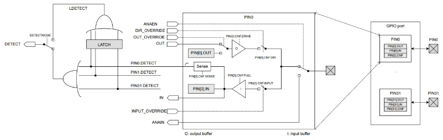
The nRF52 GPIO peripheral is responsible for managing the input and output of digital signals to and from the GPIO pins.This is a placeholder for the reference: fig-nrf52-gpio-port-pin-internal-architecture shows the internal architecture of a GPIO pin on the nRF52 series MCU.
Each MCU has one or more GPIO ports, and each port can support up to 32 GPIO pins.
GPIO Drive Strength
The GPIO pins can be configured in two different drive strengths, standard drive and high drive. This is a placeholder for the reference: tbl-nrf52-gpio-pin-current-limits shows the current limits for the GPIO pins when configured in standard drive and high drive. The current limits depend on the supply voltage and are also characterized for different output levels (e.g. 0.4 V is considered the max. for a logic low).
| Parameter | Description | Min | Typ | Max | Unit |
|---|---|---|---|---|---|
| Current at +0.4 V, output set low, standard drive, ≥ 1.7 | 1 | 2 | 4 | mA | |
| Current at +0.4 V, output set low, high drive, ≥ 2.7 V | 6 | 10 | 15 | mA | |
| Current at +0.4 V, output set low, high drive, ≥ 1.7 V | - | 3 | - | mA | |
| Current at -0.4 V, output set high, standard drive, ≥ 1.7 | 1 | 2 | 4 | mA | |
| Current at -0.4 V, output set high, high drive, ≥ 2.7 V | 6 | 9 | 14 | mA | |
| Current at -0.4 V, output set high, high drive, ≥ 1.7 V | - | 3 | - | mA |
Each pin is configured via the PIN_CNF register. There is a PIN_CNF register for every pin, available via the NRF_P[n] register (where n can be in the range 0-31). The following things can be configured:
- Direction (i.e. input or output)
- Drive strength (this includes settings for wired-and and wired-or buses)
- Enabling of pull-up/pull-down resistors
- Pin sensing
- Input buffer disconnect
- Analogue input (only supported for specific analogue capable pins)
The PIN_CNF registers are retained registers which mean they retain their values in the lowest power mode, System OFF. By default, all pins are configured as inputs but with their input buffer disabled (i.e. they are floating, and you can’t read them from firmware without first enabling the input buffer).
Input Pins
To read the state of pin P0.4:
uint32_t pin_state = (NRF_P0->IN >> 4) & 1UL; // Read the state of P0.4Output Pins
To configure a pin as an output, set the direction to output and the input to disconnect:
NRF_P0->PIN_CNF[10] = (GPIO_PIN_CNF_DIR_Output << GPIO_PIN_CNF_DIR_Pos) | (GPIO_PIN_CNF_INPUT_Disconnect << GPIO_PIN_CNF_INPUT_Pos);For output pins, write 1 to the OUTSET to set the pin high, and write a 1 to the OUTCLR to set the pin low.
NRF_P0->OUTSET = (1 << 10); // Set P0.10 highNRF_P0->OUTCLR = (1 << 10); // Set P0.10 lowOr alternatively, you can write to the OUT register to set all output pin states in one go:
NRF_P0->OUT = (1 << 10) | (1 << 13); // Set P0.10 and P0.13 high, everything else lowBe careful as OUT sets all pins. If you only want to modify the state of some, you will have to read their current value first and use |= or &=~ to set or clear the bits (a.k.a read-modify-write). OUTSET and OUTCLR are generally preferred over OUT as you don’t need to read the current state of other pins to just set or clear a single pin.
When using the Zephyr framework for writing firmware, Zephyr provides nRF specific GPIO flags for controlling the drive strength. The drive strength is individually configurable for both a logic low and a logic high output. This is done with the following macros, which set the upper 8 bits of the gpio_dt_flags_t struct:3
NRF_GPIO_DRIVE_S0: Logic low, standard driveNRF_GPIO_DRIVE_H0: Logic low, high driveNRF_GPIO_DRIVE_S1: Logic high, standard driveNRF_GPIO_DRIVE_H1: Logic high, high drive
These flags are defined in the Zephyr repo under zephyr/include/zephyr/dt-bindings/gpio/nordic-nrf-gpio.h. For example, the following code is used to configure a GPIO pin with high drive in both directions using the gpio_pin_configure_dt() function:
#include <zephyr/drivers/gpio.h>#include <zephyr/dt-bindings/gpio/nordic-nrf-gpio.h> // Needed for the NRF_GPIO_DRIVE_H0H1 macro
// Update the PATH according to your .dts file(s)const struct gpio_dt_spec l_myGpio = GPIO_DT_SPEC_GET(DT_PATH(outputs, myGpio), gpios);
int main() { // Configure the GPIO pin as output, defaulting to low, with high drive in both directions. Other flags can be ORed in here too as needed. int intRc = gpio_pin_configure_dt(&l_myGpio, GPIO_OUTPUT_INACTIVE | NRF_GPIO_DRIVE_H0H1); __ASSERT_NO_MSG(intRc == 0);}Sense and Detect
The nRF52 GPIO peripheral supports a configurable sense and detect feature which can be used to latch a register bit when the port peripheral detects a pin in a specific state. The latch is only cleared when the CPU clears it.
Pull-up/Pull-down Resistors
Every GPIO pin on the nRF52 has configurable internal pull-up and pull-down resistors. Both the pull-up and pull-down resistors have a typical value of 13kΩ, with a min. of 11kΩ and a max. of 15kΩ. The pull-up and pull-down resistors can be enabled or disabled individually per pin.2
Use the NFC Pins
By default, you won’t be able to use the two NFC pins (NFC1 and NFC2) on the MCU as GPIOs. To allow them to be used as GPIOs, add nfct-pins-as-gpios to your .dts file as shown:
&uicr { nfct-pins-as-gpios;};&uicr might already be present in your dts file with nfct-pins-as-gpios; applied. The old way of overriding the default NFC behaviour was by adding the Kconfig value CONFIG_NFCT_PINS_AS_GPIOS=y to your prj.conf. However this is now deprecated.
Successive Approximation ADC (SAADC)
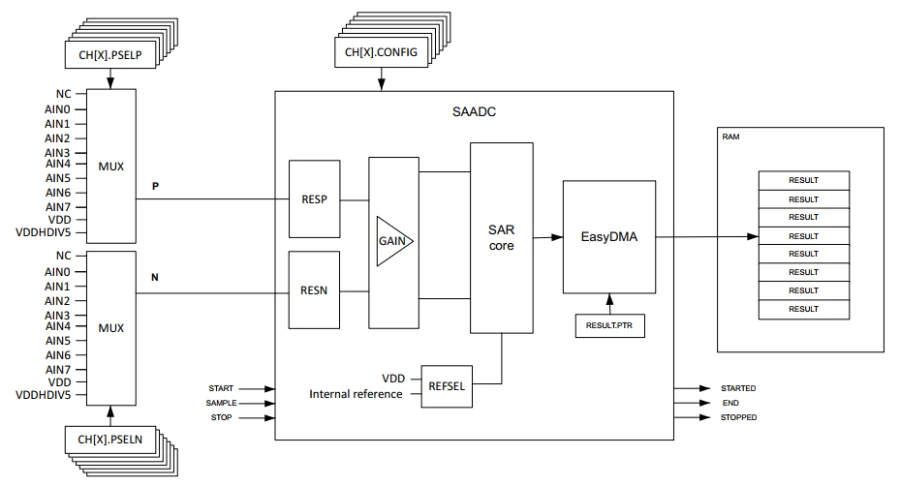
The nRF52 series MCUs have a 12-bit successive approximation ADC peripheral called SAADC. This peripheral can be used to convert analogue voltages on the AIN0-AIN7 pins to digital values. It can be used in single ended mode or differential mode. This is a placeholder for the reference: fig-saadc-internal-block-diagram-nrf52 shows the internal block diagram of the SAADC peripheral.
The accumulator in the SAADC can be used to find the average of multiple samples (oversampling). This is used to improve the SNR of the data. Oversampling can be configured with the OVERSAMPLE register. 2^OVERSAMPLE samples are averaged together before one result is written to memory. The DONE event is triggered for each input sample, and the RESULTDONE event is triggered once per averaged sample written to memory.
SAADC uses EasyDMA to write conversion results to RAM memory.
The SAADC peripheral cannot generate events when the converted value crosses a threshold. If you need this functionality, look at using the comparator peripheral (COMP) instead. The same analog input pin cannot be used for both SAADC and COMP peripherals at the same time.
Zephyr’s ADC driver can work with the SAADC peripheral. However, only basic functionality is provided by the Zephyr ADC API. For example, the Zephyr ADC API does not allow you to setup repeated sampling based on a timer connected with the DPPI/PPI. If you want more functionality than what the Zephyr ADC API provides, you can use the lower level nrfx SAADC driver.
A SAADC has a configurable acquisition time, which sets how long the input is connected to the ADC’s internal sample and hold capacitor. Inputs with a higher source impedance will require longer acquisition times to let the capacitor fully charge (and settle) to the input voltage. Acquisition times can be set using the ACQTIME register. The TACQ field in the CH[n].CONFIG register sets the acquisition time. The supported acquisition times are:2
| TACQ [µs] | Maximum Source Resistance [kΩ] |
|---|---|
| 3 | 10 |
| 5 | 40 |
| 10 | 100 |
| 15 | 200 |
| 20 | 400 |
| 40 | 800 |
Comparator (COMP)
The nRF52 series MCUs have a comparator peripheral called COMP. Much like discrete analogue comparator ICs, this peripheral can be used to compare one input voltage (VIN+) against another input voltage (VIN-), and can generate events (e.g. raise an interrupt) depending on the result (whether it is higher or lower than the other). VIN+ can be any of the analog input pins AIN0-AIN7. VIN- can be any of the analog input pins (differential mode) or from VREF, which in turn can be derived from VDD, AIN0-AIN7, or internal 1.2V, 1.8V or 2.4V references. It’s internal block diagram is shown in This is a placeholder for the reference: fig-comparator-diagram-nrf52.
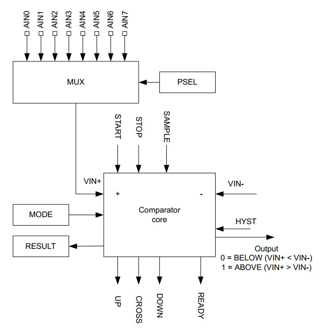
Events can be generated from:2
UPonVIN->VIN+DOWNonVIN-<VIN+CROSSonVIN-crossingVIN+READYevent when core and internal reference are ready.
These built-in events make comparator great for simple analogue change detection. The ADC peripheral (SAADC) does not have these events, so if using an ADC instead you would need to continuously poll the ADC result and compare it using CPU time (which would both be higher power and a potential waste of CPU processing time).
The comparator peripheral has configurable hysteresis to prevent false events due to noise on the inputs. In differential mode, the hysteresis is set through the HYST register and can either be set to disabled or a fixed 50mV. In single ended mode, hysteresis can be set using VUP and VDOWN thresholds. The up and down thresholds in single ended mode offer much more flexibility than the HYST register available in differential mode.
The comparator peripheral has different speed modes, which also determine the power consumption. The speed modes are set using the MODE register. The different modes are:
- Low-power mode
- Normal mode
- High-speed mode
Near Field Communication Tag (NFCT)
The nRF52 series MCUs have a near field communication (NFC) tag peripheral called NFCT. This peripheral can be used to implement an NFC tag. It supports NFC-A listen mode operation at 13.56MHz and a bitrate of 106kbps.2
This is a placeholder for the reference: fig-nrf52-nfct-peripheral-block-diagram shows the internal block diagram of the NFCT peripheral.
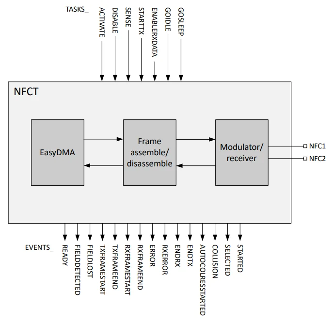
The NFCT peripheral uses EasyDMA for the reading and writing of data packets to and from RAM.
As of May 2025, Nordic has the following firmware code examples relating to NFC:4
- NFC - Launch App: Launches an app on a polling smartphone.
- NFC - Text record: Exposes a text record to polling devices.
- NFC - Shell: Runs the shell interface with the NFC T4T ISO-DEP transport layer. It uses the NFC shell transport library.
- NFC - System OFF: Wakes the MCU up from System OFF mode when it detects an NFC field.
- NFC - Tag reader: Makes the MCU a tag reader which can interact with a NFC-A tag.
- NFC - TNEP poller: Uses the TNEP for polling device library to exchange data using an NFC polling device.
- NFC - TNEP tag: Uses the TNEP for tag device library to exchange data using NFC’s TNEP Protocol on an NFC Tag device.
- NFC - Writable NDEF message: Exposes an NDEF message that can be overwritten with any other NDEF message by an NFC device.
Internal RC Oscillator
To enable the internal RC oscillator, add the following to your prj.conf file:
CONFIG_CLOCK_CONTROL_NRF_K32SRC_RC=yBy default, CONFIG_CLOCK_CONTROL_NRF_K32SRC_RC_CALIBRATION=y is set which means the calibration parameters will be used to make the RC oscillator more accurate.
Quad Serial Peripheral Interface (QSPI)
The QSPI peripheral is designed to communicate with external SPI flash memory ICs. It supports single, dual and quad lane SPI buses with a 2-32MHz clock speed. It supports Execute-In-Place (XIP) to allow the CPU to directly execute code from flash memory. This is a placeholder for the reference: fig-nrf52-qspi-block-diagram shows the internal block diagram of the QSPI peripheral.
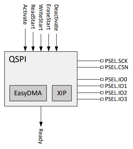
The QSPI peripheral supports a deep power-down mode (DPM) to minimize current consumption when the QSPI peripheral is not in use.
Pulse Width Modulation (PWM)
The nRF52 MCU series has a pulse width modulation (PWM) peripheral that can be used to generate PWM signals. It can be used to control the brightness of LEDs, the speed of motors, and other applications.
Firstly, it is recommended to setup the pin routing with PSEL.OUT[n] prior to enabling the PWM with the ENABLE register. This is to ensure the pins are in the correct state when the PWM is enabled. Each PWM peripheral has 4 output channels which can be routed to any of the GPIO pins.
NRF_PWM0->PSEL.OUT[0] = 10; // P0.10NRF_PWM0->PSEL.OUT[1] = 0xFFFFFFFF; // Disconnect channel 1NRF_PWM0->PSEL.OUT[2] = 0xFFFFFFFF; // Disconnect channel 2NRF_PWM0->PSEL.OUT[3] = 0xFFFFFFFF; // Disconnect channel 3Then enable the peripheral with the ENABLE register:
NRF_PWM0->ENABLE = PWM_ENABLE_ENABLE_Enabled << PWM_ENABLE_ENABLE_Pos;Then you can set the operating mode of the wave counter with the MODE register. The different modes are:
Up(default): The wave counter counts up from 0 to theCOUNTERTOPvalue. Generates edge-aligned duty cycles.UpAndDown: The wave counter counts up from 0 to theCOUNTERTOPvalue, and then down to 0. Generates center-aligned duty cycles.
For example, to set the operating mode to Up:
NRF_PWM0->MODE = (PWM_MODE_UPDOWN_Up << PWM_MODE_UPDOWN_Pos);Use the COUNTERTOP register to set the maximum value the pulse generator counts to. This, along with PRESCALER to set the PWM clock frequency, is how you set the PWM frequency. The value written to this has to be in the range [3, 32767]. It defaults to 0x3FF. For example, to set the PWM frequency to 100kHz when the PRESCALER is 0:
NRF_PWM0->COUNTERTOP = 160; // Assuming PRESCALER is 0, then the PWM frequency is 16MHz / 160 = 100kHzCOUNTERTOP can be safely written to at any time. It is sampled following a START task.
Use the SHORTS register to make certain events automatically trigger tasks. Note that the chaining of sequence 1 after sequence 0 is implicit.
PTR is where you write a pointer to the buffer you want the PWM to read out duty cycles (and potentially also PWM period) from. The buffer must be word aligned (i.e. 4 byte aligned since it’s a 32-bit architecture). Each element in the buffer is a 16-bit value. The MSB sets the polarity of the output. 0 is RisingEdge and 1 is FallingEdge. This is in reference to the edge which occurs when the counter equals the duty cycle value in the PTR buffer. If you are driving an output that is active high, you probably want to set the MSB to 1 so that the duty cycle sets how long the output is high for in a period, rather than how long it is low for.
// Configure pin routingNRF_PWM0->PSEL.OUT[0] = 10;  // P0.10NRF_PWM0->PSEL.OUT[1] = 9;   // P0.9NRF_PWM0->PSEL.OUT[2] = 0xFFFFFFFF;  // Disconnect channel 2NRF_PWM0->PSEL.OUT[3] = 0xFFFFFFFF;  // Disconnect channel 3
// Enable PWM0NRF_PWM0->ENABLE = PWM_ENABLE_ENABLE_Enabled << PWM_ENABLE_ENABLE_Pos;
// Configure PWM parametersNRF_PWM0->PRESCALER = 0;  // 16MHz / 2^0 = 16MHz clockNRF_PWM0->COUNTERTOP = 160;  // 16MHz / 160 = 100kHz PWM frequencyNRF_PWM0->MODE = 0;  // UP counter modeNRF_PWM0->DECODER = 0;  // Individual decoding, grouped loading, 16-bit valuesNRF_PWM0->LOOP = 0;  // Loop disabled (continuous)
pwm_buffer[0] = 160;  // P0.10 - 100% duty (full on)pwm_buffer[1] = 136;  // P0.9 - 85% duty
// Configure sequence 0NRF_PWM0->SEQ[0].PTR = (uint32_t)pwm_buffer;NRF_PWM0->SEQ[0].CNT = 2;  // 2 values (P0.10, P0.9)NRF_PWM0->SEQ[0].REFRESH = 0;NRF_PWM0->SEQ[0].ENDDELAY = 0;
// Start PWM sequenceNRF_PWM0->TASKS_SEQSTART[0] = 1;
Pin Configuration
Before configuring the pin in the PWM peripheral, the Nordic documentation states that you should configure the pin in the GPIO peripheral first.
// Configure P0.10 as GPIO output, always HIGHNRF_P0->PIN_CNF[10] = (1 << 0) | (0 << 1); // DIR=output, INPUT=disconnectNRF_P0->OUTSET = (1 << 10); // Set P0.10 HIGHThe idle state of a pin is defined by the OUT register in the GPIO module, to ensure that the pins used by the PWM module are driven correctly. If PWM generation is stopped by triggering a STOP task, the PWM module itself is temporarily disabled or the device temporarily enters System OFF. This configuration must be retained in the GPIO for the selected pins (I/Os) for as long as the PWM module is supposed to be connected to an external PWM circuit.2
Dithering
The nRF52 PWM peripheral supports temporal dithering to artificially increase the resolution of the PWM. This is where you vary the duty cycle between two adjacent discreet duty cycle values (on a cycle-by-cycle basis) to give the appearance of a higher resolution PWM. This is achieved by using the sequence feature in the PWM peripheral (which can be used for more than just dithering).
From testing, it appears you can’t loop continuously over a single sequence, you always need to setup and use the two sequence registers.
For more information on dithering, see the PWM dithering section.
Jumping From Bootloader to Application
Sometimes you may need to initialize a PWM peripheral in the bootloader and leave it running when jumping to the application. This will work as long as you make sure there is not initialization code in the app which resets the peripheral, and also that the buffer you pass to the peripheral (via the PTR register) is not overwritten by the application. To prevent the buffer from being overwritten, you typically have to reserve some RAM which is shared between the bootloader and the application and is not part of the bootloader/application heap/stack.
Timer/Counter (TIMER)
The nRF52 series MCUs have a standard timer/counter peripheral called TIMER. This peripheral can be used to generate interrupts and events based on a timer counter compare value. They are useful for generating periodic events (e.g. a system tick) and for measuring time intervals.
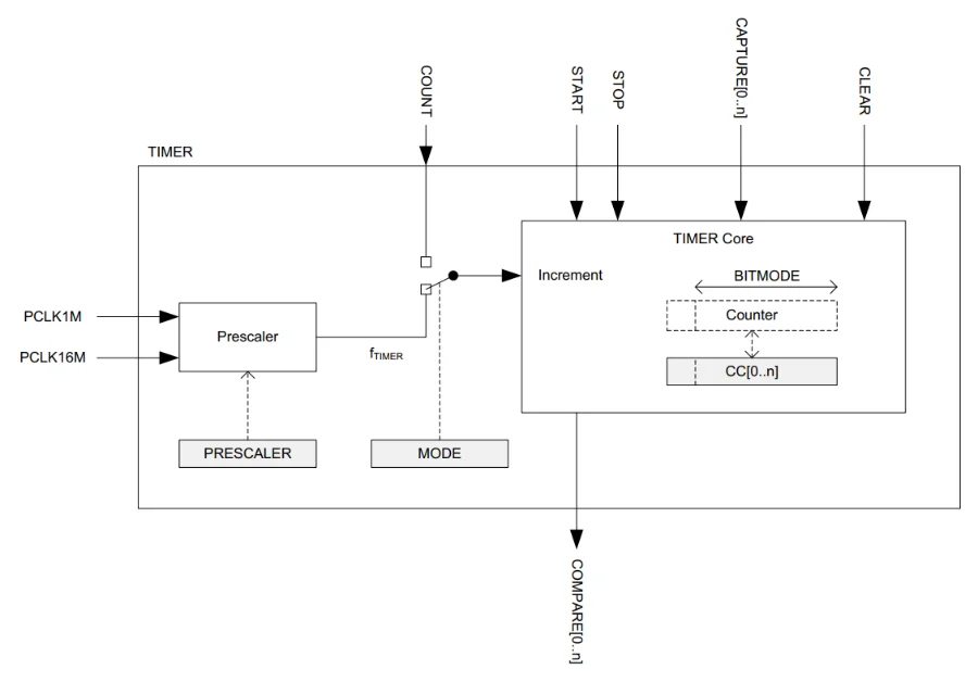
Unlike peripherals such as the PWM, the TIMER does not have an ENABLE register. Write a 1 to the TASKS_START register to start the timer/counter:
NRF_TIMER0->TASKS_START = 1;Write a 1 to the TASKS_STOP register to stop the timer/counter (but make sure to note the errata below!):
NRF_TIMER0->TASKS_STOP = 1;Watchdog Timer (WDT)
The nRF52 series MCUs have a watchdog timer peripheral called WDT. This peripheral can be used to reset the MCU if it becomes unresponsive. WDT always uses a 32.768 kHz clock source. It will automatically enable the internal 32.768 kHz RC oscillator as long as no other 32.768 kHz clock source is generating the 32.768 kHz system clock.
The WDT peripheral does not have an ENABLE register like many of the other peripherals.
Here the bare minimum needed to configure and start the WDT:
NRF_WDT->CRV = 32768*10 - 1; // 10s timeout (32.768kHz WDT clock)NRF_WDT->TASKS_START = 1;Without doing anything more, the WDT will reset the MCU 10 seconds after calling NRF_WDT->TASKS_START = 1;.
To prevent the watchdog from resetting the MCU, you need to feed it by writing a special value to the reload request register. The value is 0x6E524635.
NRF_WDT->RR[0] = 0x6E524635;The RR[0] register is the only reload request register enabled by default. There are eight in total that can be enabled. The watchdog only reloads it’s counter value when all enabled reload request registers have been written to. This enables you to implement a more complex watchdog mechanism by having different threads write to different reload request registers. If any thread fails to perform it’s reload request, the watchdog will reset the MCU. For more than 8 threads, you can implement a software watchdog which is responsible for monitoring the threads and writing to the single reload request register if all threads are ok.
The RREN register can be used to enable and disable reload request registers:
NRF_WDT->RREN = (1 << 0) | (1 << 1) | (1 << 2); // Enable reload request registers 0, 1 and 2The CONFIG register can be used to configure whether the WDT is paused in sleep and when the CPU is halted by the debugger. By default the WDT is not paused in sleep and is paused by the debugger.
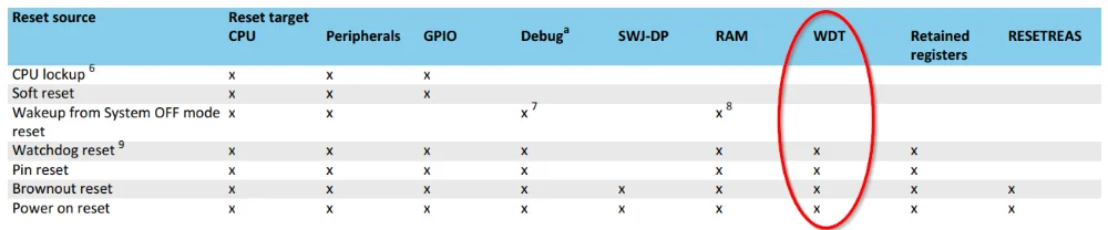
NRF_WDT->CONFIG = (1 << 0) | (1 << 1); // Pause in sleep, pause by debuggerThe watchdog must be configured before it is started. This means you must setup the CRV, RREN and CONFIG registers as desired before calling NRF_WDT->TASKS_START = 1;. After starting the watchdog, these configuration registers cannot be changed (this is to prevent the watchdog from accidentally being disabled by malformed code that just happens to write to those memory addresses). The only way to reconfigure a watchdog once started is to reset. The reset source must be a watchdog reset, pin reset, brownout reset or power on reset. CPU lockup, soft reset (a software reset — setting the SYSRESETREQ bit of the application interrupt and reset control register (AIRCR register)) and wakeup from System OFF mode do not reset the watchdog.
You can use the INTENSET register to enable the TIMEOUT interrupt. This interrupt is triggered when the watchdog timer expires. If the timeout event is enabled, the WDT peripheral delays the MCU reset by two 32.768 kHz clock cycles to give you a small window of time to react to the event in firmware before the reset. It appears that unlike the main configuration registers, the interrupt can be configured after the watchdog has started (which make sense as you cannot disable the watchdog by enabling the interrupt — only delay the reset by a small amount).
Footnotes
-
Nordic Semiconductor. Products / nRF52840 [product page]. Retrieved 2025-03-03, from https://www.nordicsemi.com/Products/nRF52840. ↩ ↩2 ↩3
-
Nordic Semiconductor (2024, Oct 1). nRF52840 - Product Specification - v1.11 [datasheet]. Retrieved 2025-03-03, from https://docs.nordicsemi.com/bundle/ps_nrf52840/page/keyfeatures_html5.html. ↩ ↩2 ↩3 ↩4 ↩5 ↩6 ↩7 ↩8 ↩9 ↩10 ↩11 ↩12 ↩13 ↩14
-
Zephyr Project (2025, Mar 3). Device Driver APIs > GPIO Driver APIs > nRF-specific GPIO Flags [documentation]. Retrieved 2025-03-03, from https://docs.zephyrproject.org/apidoc/latest/group__gpio__interface__nrf.html. ↩
-
Nordic Semiconductor (2025, May 7). nRF Connect SDK - latest > Samples > NFC samples [documentation]. Retrieved 2025-05-08, from https://docs.nordicsemi.com/bundle/ncs-latest/page/nrf/samples/nfc.html. ↩
-
Alex_S@Aperia, Vidar Berg. Unable to pull SPI MISO line down via device tree configuration [forum post]. Nordic Semiconductor DevZone. Retrieved 2026-01-16, from https://devzone.nordicsemi.com/f/nordic-q-a/113908/unable-to-pull-spi-miso-line-down-via-device-tree-configuration. ↩
-
Nordic Semiconductor (2024, Mar 4). nRF52832 Revision 3 Errata. Retrieved 2026-02-20, from https://docs.nordicsemi.com/bundle/errata_nRF52832_Rev3/page/ERR/nRF52832/Rev3/latest/err_832.html. ↩ ↩2