The PCB Rework Guide
Get a Good Quality Soldering Iron
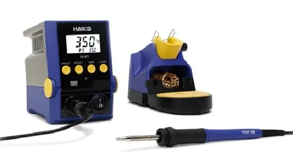
Your soldering iron is going to be the most important tool when performing PCB rework. Make sure you have a good quality one! You want one that has good temperature control, and supports a range of quick-change tips. You will want a selection of tips, from large chisel tips for heating up large pads or bits with thermal relief, to fine angled tips for delicate work.
The Hakko FX-971 soldering iron shown in This is a placeholder for the reference: fig-hakko-fx-971-soldering-iron is an example of a soldering iron suitable for PCB rework.
Magnification
It today’s age with SMD components being so small, some form of magnification tool is essential for fine work. I find I can solder down to about 0402 chip size with the naked eye, but need magnification when soldering on things like 0.65/0.50mm pitch leads.
One of my favourite magnification tools is a magnifying lamp that can be clamped to your desk, as shown in This is a placeholder for the reference: fig-magnifying-lamp-desk-clamped. I prefer the clamp style rather than the heavy base style, as it doesn’t take up as much desk space and is more secure. Most come with a ring of LED lights to illuminate the work area (sometimes adjustable in brightness).

Lead-Based Soldering
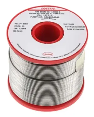
Although lead-free solder should be used for production PCBs, lead-based soldering is ok for small amounts of prototype rework. Leaded solder is almost always easier to work with compared to it’s lead-free counterparts. It typically has a lower melting point, and flows more easily. These are vital properties if you are doing a spot of tricky rework.
Kapton Tape IC Pin Swap Method
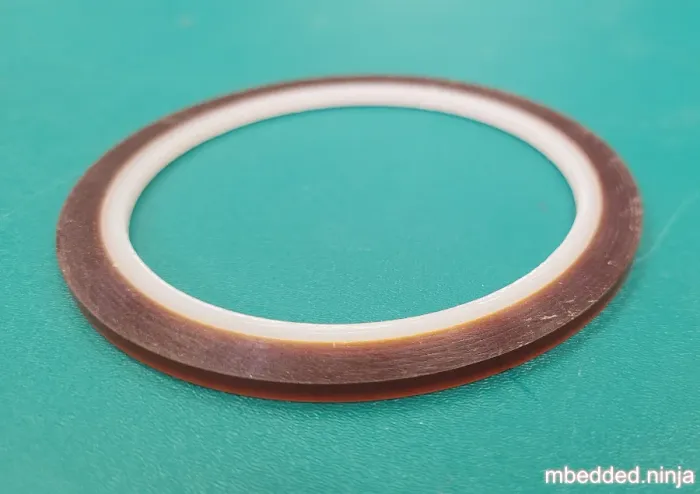
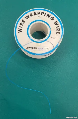
Sometimes you might realize you have wired up the pins of an IC incorrectly, and some of them need rerouting for the circuit to work. One technique to do this is to place Kapton tape under the leads of the IC to insulate them from the PCB pads, and then reroute them to other parts of the circuit using hook-up wire.
This method works well if:
- The IC has leads that protrude from the body of the IC. For example, SOIC, TSSOP, QFP, SOT. Packages where this doesn’t work well is ones which only have pads on the side of the IC, e.g. QFN or DFN. Totally impossible if the pads that need rewiring are on the underside of the IC, e.g. BGA or LGA.
- Some of the pins don’t need rewiring, and can act as anchor points for the IC.
- There are no high current or thermal concerns due to rewiring some of the pins with wire wrap wire (if there is concerns, you might need to just respin the board!).
- There are other solderable parts on the PCB (e.g. pads of chip resistors/capacitors, other IC pins, test points, e.t.c.) that you can reroute the pins to.
Firstly, remove the IC from the PCB (if it was soldered on prior to you realizing your mistake). This could be done with a hot air gun to remove the IC. Then remove the leftover bits of the solder from the pads. This could be done with copper braid and a soldering iron (remember to add a bit of flux to the braid to boost its solder sucking ability).
Next, clean up any flux residue from around the pads (e.g. with isopropyl alcohol), because we want the Kapton tape to stick well.
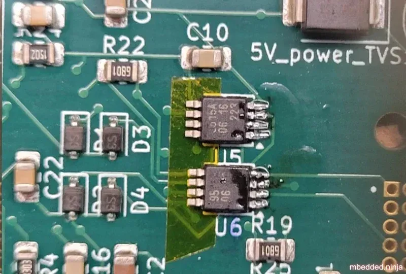
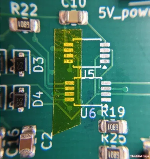
Then, cut a piece of Kapton tape to size and place it over the pads you need to swap around as shown in This is a placeholder for the reference: fig-kapton-tape-ic-pin-swap-tape-over-pads.
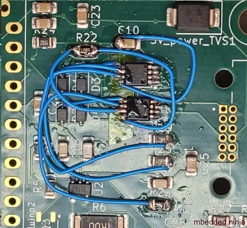
Next, solder the IC back in place using the pins that don’t need swapping, as shown in This is a placeholder for the reference: fig-kapton-tape-ic-pin-swap-ics-soldered-back-on.
Now you need to connect the pins that need rewiring to other parts of the circuit. If you have a small pitch IC (e.g. 0.5-0.65mm) you might need a magnifying lamp or similar optical aid to tack the wires in place.
Cleaning Up Flux Residue
You may or may not want to clean up the flux residue after the rework is complete. Modern fluxes don’t typically cause long term problems if left on the board (plus, it it’s just a prototype, longevity might not be a concern). So it’s usually more a matter of appearance, as the left over flux can be quite unsightly.
If you do want to clean up the flux residue, one of the best ways is to dunk it in an ultrasonic bath. If you don’t have one (or if you can’t, because there is something on the PCB which wouldn’t like being submerged), then isopropyl alcohol and a cotton bud will work. Apply some isopropyl alcohol and gently scrub with the cotton bud to loosen/dissolve the flux residue. Then flush the area with more isopropyl alcohol so that is “washes” the dissolved residue away (I let it drip on the floor).
Too Much Rework
Be careful, this is such a thing as too much rework. After many heat cycles and physical stress, things can start wearing out, such as:
- Copper pads on the PCB lift off (delaminate).
- Small parts of solder mask flake off.
- Oxidization makes it harder for the solder to flow, resulting in cold/dry joints (flux goes a long way to fixing this).
Cutting Tracks
You might need to cut tracks on a PCB to change the routing of a net. If the track is on the bottom or top layer of the PCB (and not underneath a component), not too short and not spaced too closely to other tracks, you can normally cut them quite easily with a sharp knife or scalpel.

You won’t be able to cut it in a single stroke, so you need to make a series of cuts. Think of it sort of like scratching of the surface. You will first cut through the soldermask and see shiny copper. Then with some more cutting you should a change in the texture as you hit the fibreglass substrate underneath. Inspect that you have cut through the entire track with a magnifying glass, or use a continuity tester if possible.
If the track is on an inner layer, there is no really good way to cut it! If there is no critical copper directly above or below it in the stack-up, you could try drilling a hole through the entire PCB to break the connection. It is hard to locate the drill bit correctly, and you run the risk of creating shorts between layers if some of the copper is not cut cleanly and shears down the side of the hole. Drilling out a via to break a connection is another option.


