Pads, Vias And Holes

Holes
Holes in PCBs are typically used to mount through-hole components (their main use), and to provide places to secure the board mechanically. Holes are typically plated (which makes them identical to vias), but non-plated also have their uses (e.g. mounting or connector location holes). Holes with copper rings have to obey the minimum annular ring size clearance. Most PCB manufacturers will have a pricing regime that is dependent on the smallest hole size used, the total number of holes, and also the number of different hole sizes.
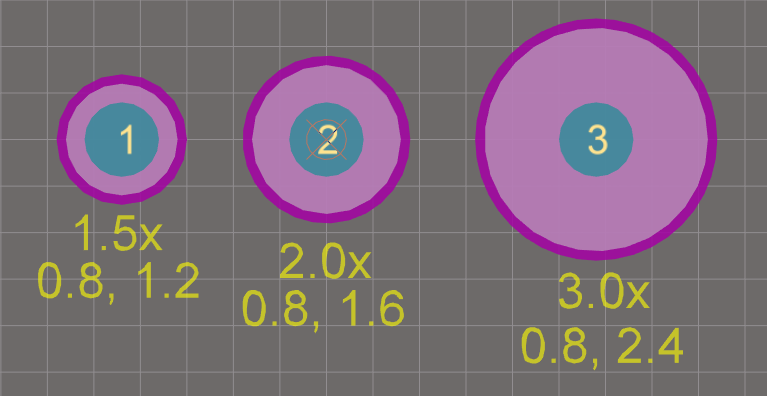
The smallest hole PCB manufacturers can support is usually 0.1-0.2mm, with anything under 0.2mm becoming specialty and hence more expensive. Holes which are designed for component leads to go through require pads surrounding the holes on the top and/or bottom of the PCB. This allows a good solder bond between the component and the PCB tracks. A typical rule-of-thumb is to make the pad diameter twice the size of the hole diameter. The middle pad in the image below shows this.
Vias
Vias are simply the name given to plated holes which are used to connect to tracks on different layers rather than to mount through-hole components (remember that holes are primarily used to mount through-hole components, but also can connect tracks on different layers).
Current-Carrying Ability
DESIGN TIP: As a rule of thumb, a via with a certain diameter can carry 3 times as much current than a track with the same width.
The above rule-of thumb stems from the fact that when a via wall is unrolled into a 2D track shape, it would be wide (), where is approximately equal to 3. This assumes that the via wall is the same thickness as the copper track (e.g. 32um or 1oz. copper)). This does not take into account the difference between an external track and a via which is surrounded by PCB material. Since PCB material is more thermally conductive than air, this rule is on the safe side.
Via Current Calculator
Use the calculator below to find the IPC-2221A maximum current, cross-sectional area, electrical resistance and thermal resistance of a via.
Drilling Out Vias
Vias can be drilled out easily to break connections when re-wiring, modifying existing PCBs. Just use a drill-bit 2-5x the diameter of the via’s copper pad, and drill down gently until the connection between the via’s pad and plated hole are disconnected.
Microvias
Microvias are tiny vias that are usually characterised by a diameter of 150um or less (this is the formal IPC definition). At these diameters, the vias cannot be formed with standard drill bits. Other forms of technology have to be used. These include:
- Photovias
- Laser Vias
Microvias are used extensively as part of via-in-pad technology, in where the via is placed directly on the pad of a component, compared to placing it beside the pad a running a short copper track to it. This offers significant space reductions in high-density PCBs.
Microvias are part of the technology set that make up HDI (High-Density Interconnect) PCBs.
The advantage of additive and semi-additive PCB design processes is that microvias can be drilled prior to plating the surface.
Laser Vias
Trepanning is when the laser is moved in a circular pattern to make a large diameter via.
CO2 Laser Only: Shadow mask method with CO2 laser. An opening is etched into the copper lyaer. Then the CO2 laser burns the dielectric material down to the first inner layer.
UV/CO2 Laser: (approx. 200 drill holes per second). The outer copper layer is removed by the UV laser, then the CO2 layer removes the dielectric.
UV Laser Only: Approx. 80 drill holes per second. UV laser removes both copper and di-electric laser.
Annular Rings
The annular ring is the width of the copper pad which surrounds the via/pad hole.
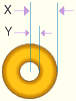
Most PCB manufacturers specify a minimum annular ring distance, and may offer more expensive pricing tiers for smaller minimum annular rings. The minimum annular ring is typically driven by the accuracy in which the PCB manufacturer can drill the via/pad hole. The drill hole may wander from the desired center in the x and y direction, and they need a specify a minimum annular ring to guarantee there will always be a copper pad surrounding the drilled hole. If the drill hole touches the side of the copper pad (i.e. the annular ring reduces to 0), this error condition is called tangency. If the problem is even worse and the drill hole escapes the pad, this is called breakout1.
Typical minimum annular rings for standard commercial PCB manufacture is between 0.1-0.15mm (3.94 to 5.91mill). Coupled with a typical minimum hole size of 0.2mm, this puts the minimum via/pad size at 0.2mm + 0.1mm*2 = 0.4mm.
Direct Connect Vs. Thermal Relief
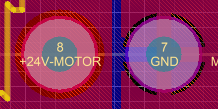
Thermal relief is a connection style between copper pours (typically power or ground pours) and other copper elements on the PCB connected to the same net (typically component pads, although this can apply to vias also). A four-point connection is the most common style of thermal relief.
The image below shows a a direct-connect style pad on the left, and a thermal relief style pad on the right.
Component pads without thermal relief can tombstone upon cooling. If one pad is solidly connected to a copper plane, while the other pad is connected to a thin track, the solidly connected pad will cool much faster after soldering. This can cause the pad to pull the component closer (due to surface tension) and pull the component off the other pad, even raising it so the component is standing on its end (tombstoning). This can be somewhat mitigated with slow changing, controlled temperature profiles in a reflow soldering environment.
Component removal and rework can be difficult with components without thermal relief pads.
Thermal relief can starve pads. This occurs when there are many other tracks routed close to a pad with thermal relief connections. While a four-point connection is desired, three of these four connection points may be inhibited due to tracks belonging to other nets.
When Direct Connect Wins
Thermal relief gives way however to important considerations such as current capability and signal integrity. It is often a difficult decision on whether a pad or via should be directly connected to a copper plane, or whether thermal relief should be provided.
It is common to see power converter (e.g. SMPS) designs that forgo thermal relief in favour of direct connections on the high current pathways. The input/output power connections to the PCB will usually have direct connections also.
Thermal Relief And Vias
You don’t need to add thermal relief to vias. If nothing is soldered to it, then all your are doing is making your connection worse. Most EDA software programs will allow you change this easily (in Altium you set up a rule).
Filled Vias
Filled vias can be broadly separated into the two categories:
- Non-conductive via filling (a.k.a resin-filled vias): The via is filled with a non-conductive resin. It is then electroplated so that copper caps form on both ends of the plug. The surface is then planerized to make it flat, before the final surface finish is applied (e.g. ENIG, HASL). Note that the via is still conductive, as before it’s plugged the standard electro-plating process is done.
- Conductive filled vias: Vias are filled with an electrically and thermally conductive material. Typically used for high performance PCB designs that need to carry a large amount of heat or current from one side of the board to the other. The conductive material typically has a specific thermal resistance of 3.5-15 W/mk.
Although the 3-15W/mK specific thermal conductivity of the filled conductive via material is much higher than a insulating conductive resin (0.25W/mK), it is still much lower than the thermal conductivity of the plated copper (which forms the barrel of the via), which is typically between 250-400W/mK. Thus conductive filled vias do not offer significant improvements over standard vias. Coupled with the large additional manufacturing costs, conductive filled vias are not a common choice for many PCB designs.
Aspect Ratios
The aspect ratio is an important parameter of a hole on a PCB. It is defined as:
The is the same as the PCB thickness if the start and finish layers of the hole are the top and bottom layers of the PCB. This is true in most cases, but will not be the case for all holes in a PCB design that uses buried or blind vias.
For example, a hole with a 0.5mm diameter going entirely through a 1.6mm thick PCB has an aspect ratio of
The maximum aspect ratio present on a PCB is an important parameter for the PCB manufacturers. Most manufacturers have an upper limit on the aspect ratio that they can manufacture reliably. This is normally about an aspect ratio of 10-12.
How To Calculate The Thermal Resistance Of Holes And Vias
See the Thermal Design For PCBs page for equations and an online calculator to work out the thermal resistance of both PCB holes and vias.
Footnotes
-
https://www.pcbdirectory.com/community/what-is-an-annular-ring, retrieved 2020-09-16. ↩