IMS (Insulated Metal Substrate) PCBs
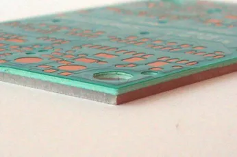
Insulated metallic substrate (IMS) PCBs are PCBs which use a metallic material as a a thick base or inner layer to improve the thermal and mechanical properties of the PCB. They are also known as aluminium base, aluminium clad, metal clad (MCPCB), or thermally conductive PCBs (ergh…bad name, all PCBs are pretty thermally conductive). A 3-10 fold thermal improvement over standard FR-4 can be achieved.
Aluminium is normally used as the substrate (with copper still being used for the electrical layers) because of it’s low cost, however copper is used in more expensive/higher power density designs because of it’s superior thermal conductivity. Copper also has a lower co-efficient of thermal expansion and is also used when the stresses on the component’s solder joints need to be reduced.
Uses
- High power applications
- Where there are large mechanical loads
- High level of dimensional stability is required
- Flammability concerns/restrictions
- Extra electromagnetic shielding is required
The increased thermal conductivity of IMS PCBs allows for higher packing densities (you can have thinner copper tracks for the same current!), longer operating times, more reliable devices (reduces thermal stress and drops the MTBF).
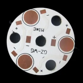
IMS PCBs are used for power LED PCBs, motor drivers. welding machines, SSRs, power conversion circuits and more.
There are also direct bonded copper (DBC) substrates, active metal braze (AMB) substrates
Sometimes using a IMS PCB saves you having to use a heatsink!
Thermal Conductivities
Just for comparison, here are the thermal conductivities of various PCB materials. Note that these units are Watts per metre per Kelvin (or Watts per metre-Kelvin).
- Copper:
- Aluminum:
- Water:
- FR4:
- Thermal prepreg:
- Still Air:
Notice how traditional PCB prepreg has a very poor thermal conductivity at .
Design
Basic ones allow for components to be placed on one side only. White and black are common soldermask and silkscreen colours for IMS PCBs. More advanced ones follow normal stack-up rules, except one or more “cores” in the PCB is replaced with a metallic material. Prepreg and normal copper layers still used. However prepreg layers are small (typically 20-100um thick), and they have poor thermal conductivity! However we can’t make the dielectric too thin or the dielectric strength will be too low (and we will get breakdowns). Special prepreg can be used that is ceramic or boron-filled to increase it’s thermal conductivity while keeping it’s insulating properties.
An IMS PCB can be plated using most common plating techniques. However, HASL is not preferred due to the uneven surface it creates compared to other processes such as Cu-OSP, immersion Sn or NiAu (ENIG).
Single-Sided, Single-Layer IMS PCB
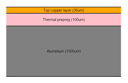
This is the most basic and cheapest IMS PCB design layout. It consists of one electrical layer sandwiched to a metallic substrate with some prepreg in-between. It is commonly used for basic high-power LED PCBs and other simple circuits which don’t require too much routing.
Single-Sided, Double-Layered IMS PCB
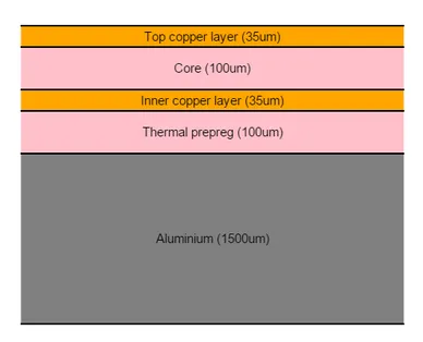
This design is not much more complex than a single-layer, single-sided IMS PCB. All it is is an extra electrical copper layer just below the top electrical layer. A thin two-layer PCB is made using the normal PCB processes, and then the metallic substrate is added to complete the PCB.
The non-component side of a 1-sided IMS PCB can be mounted to a heatsink (e.g. the device’s enclosure) for a huge decrease in the total thermal resistance of the device. Thermal interface layer (TIM) between IMS PCB and the heatsink.
Maximum dimensions seem to be around 500x500mm.
Flammability rating can be 94V0.
PCB Constraints
Depending on the design, the thermal conductivity can range from 0.60 (average to good) to 2.2W/mK (really good), where FR4 is 0.3W/mK. 1.5mm and 2.0mm are common thicknesses. I have seen 0.8, 1.0, 1.2, 1.5, 1.6 and 2.0mm supported. Copper thickness ranges from 35->200um.
Minimum conductor width: 200um
Minimum conductor spacing: 200um
Min. annular ring: 150um
Min via (pth): 0.3mm
Glass transition temp for dielectric layer: 130C
Er (permittivity): 4.2-4.7.
Thermal Management Alternatives To IMS
Moving from a traditional PCB to a IMS PCB can be quite a large design/manufacturing change. Before doing this, think, “Can I get improve the thermal properties of my PCB in any other way?”. Here are some alternatives to IMS PCBs:
- Thermal vias (note that these can be also used in conjunction with IMS PCBs)
- Thicker copper layers. 35um (1 oz.) thick copper is standard, but most PCB manufacturers allow you to increase the thickness by a large amount!


