Desmear And Etchback
The mechanical of vias in multi-layer PCBs crates a residual resin that smears along the walls of the vias, preventing a good electrical connection between the copper layers and the via itself. The residue is due the the heat of the drill bit melting the resin and smearing it across the inner-layer copper surfaces in the via barrel. The idea behind desmear is to remove this residue so that a good connection is achieved when the via is plated (metallized). Etchback is the idea that one can go further than just removing resin, and etch away some of the epoxy/resin from the via barrel wall, giving what people call a “three-point connection” which could provide even better connectivity (this is a controversial topic). This is commonly used on high reliability PCBs (such as military, aerospace and medical PCBs).
Positive Etchback
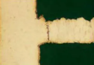
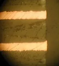
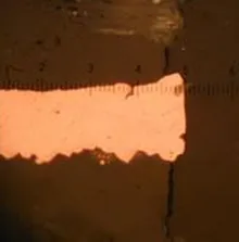
The images below show positive etchback.
Negative Etchback
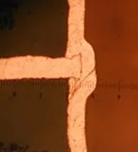
Negative etchback is when the copper layers recede from the edge of the via hole, as shown in the diagram below.

Methods
Desmear and etchback can be done with chemicals or by using plasma. The chemical process usually involves a alkaline potassium permanganate based etchant. This etchant must be completely removed before the via is plated.
The plasma method uses the creation of gaseous free radicals which attack the residue to form volatiles which can be sucked away.


