TO-268 (D3PAK) Component Package
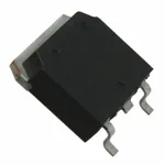
The TO-268 (Transistor Outline 268, commonly known as D3PAK) is a SMD component package. It is the third in the series of “DPAK” packages, the first being TO-252 (DPAK) and the second being TO-263 (D2PAK). The D3PAK name stands for “decawatt 3 package” and has the highest power dissipation rating out of the three. Unlike the TO-263 package, the TO-268 package only comes in one variant with 3 pins (as far as I can tell). This variant can be referred to as TO-268-3.
It is designed to have a really low thermal resistance so that it can be used in high power applications. The larger die also means that MOSFETs in this package can have lower values, resulting in less power dissipation for the same current.
I have only ever seen this in the 3-pin variant (called TO-268-3). Common uses include Microsemi power MOSFETs, Microsemi power diodes, and Microsemi power IGBTs.
Synonyms
- TO-268 (Transistor Outline 268)
- D3PAK
- DDDPAK
- Decawatt Package 3
- TO-268AA (TO-268-3)
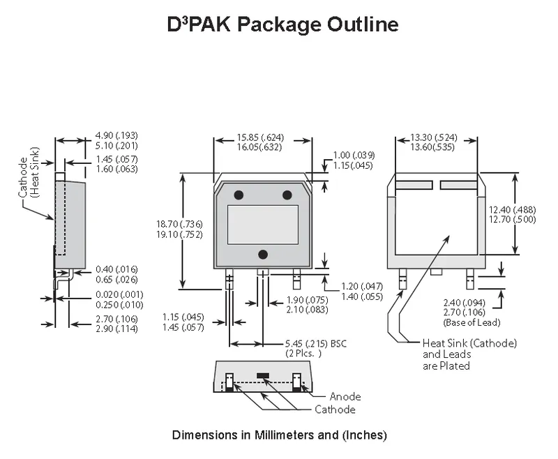
Package Dimensions
Shown below are the package dimensions.
Thermal Resistances
- (13.5x17.5mm copper pad)
- (19x29.4mm copper pad)
Solderability
Easy to solder by hand, as long as you have a decent powered soldering iron for the central thermal pad. Easy to solder with infrared and reflow techniques.
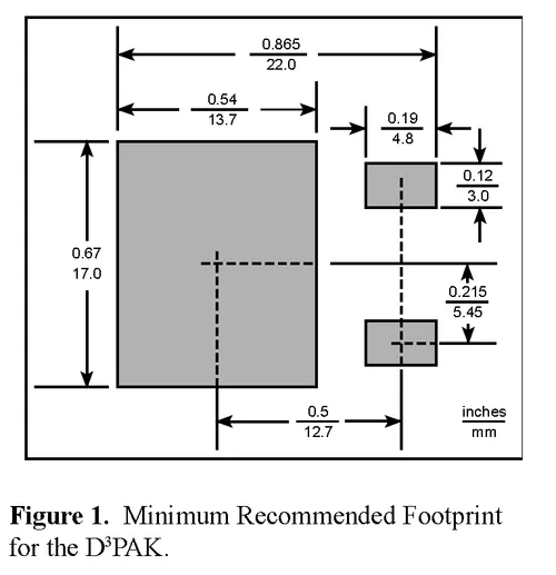
Recommended Land Pattern
Shown below is the recommended land pattern.
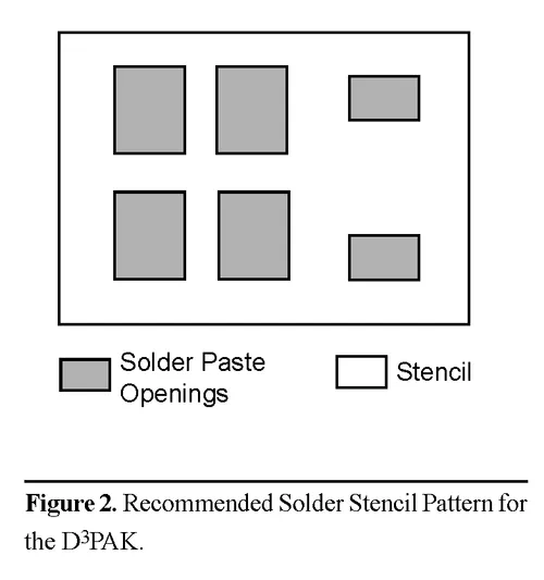
Recommended Stencil
Shown below is the recommended stencil pattern.


