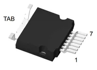
HU3PAK Component Package
The HU3PAK component package is a package design used solely by ST Microelectronics. It has 7 leads plus a tab (which has two PCB contact points). It has a pitch of 1.27mm2. It’s designed attached to a heatsink on it’s top surface, but unusually does not have any provision for thermally coupling to the PCB (the recommended footprint only has a small amount of soldering points for the 7 pins and two tab locations).
The only use I could find for this package is for MOSFETs1.
Dimensions
The HU3PACK is 14mm wide, 18.58 long (including leads) and 3.50mm high2.
Thermal Resistance
- 1
- 1 (when mounted on 2oz. 1inch^2 PCB) (note that this thermal resistance hides the fact that the thermal resistance to ambient can be much lower if a top-side heatsink is added as intended)
References
Footnotes
-
ST Microelectronics (2021, Nov). STHU32N65DM6AG: Automotive-grade N-channel 650 V, 83 mΩ typ., 37 A MDmesh DM6 Power MOSFET in an HU3PAK package (datasheet). Retrieved 2022-11-07, from https://www.st.com/resource/en/datasheet/sthu32n65dm6ag.pdf. ↩ ↩2 ↩3 ↩4
-
ST Microelectronics (2021, Nov). TN1378: HU3PAK package mounting and thermal behavior. Retrieved 2022-11-07, from https://www.st.com/resource/en/technical_note/tn1378-hu3pak-package-mounting-and-thermal-behavior-stmicroelectronics.pdf. ↩ ↩2


