Castellation
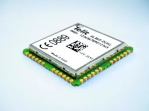
Castellation is a way of mounting one PCB onto another. It is also known by the name half-vias, edge-plating and leadless chip carrier (LCC).
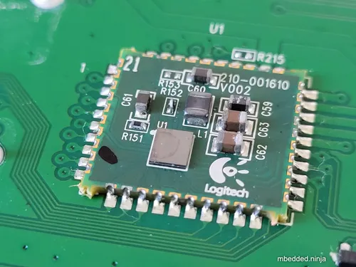
It is a common technique used for a daughter board, module or secondary PCB that needs to be mounted on the main PCB.

Once soldered onto the parent PCB, it is a permanent attachment.
Process
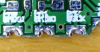
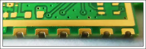
Rows of holes are drilled around the edge of the PCB. Once the holes have been through-hole plated, the board edge is cut so that it runs right down the middle of these holes. The edge of the board now looks like the top of a castle wall, hence the word castellation.
Design
- Make the vias as large as possible
- Make the top and bottom copper layer pads for the vias as large as possible
- Add pads to the castellated vias on middle layers if possible, to help anchor the barrel. This will reduce burring during the routing.
The holes can be both used for mechanical fixture and also to pass electrical signals between the main and daughter PCBs.
The holes, since on the edge of the daughter PCB, do not use up much valuable space (you normally have to have a component/track clearance around the edge of the board anyway)!
Because the half-holes are plated and of a concave shape, they are very suitable for soldering.
Watch out for torn edge-holes!

The router bit can squash the via barrels, as shown in the following image:


