KiCad Tips And Tricks

KiCad is an open-source electronic design CAD software package. It runs on Windows, Linux and MacOS.
KiCad is a C++ program which uses the wxWidgets library to provide the GUI elements.
KiCad organizes work into projects. Each project has a project file ending in .pro. A Project consists of schematics (.sch), a PCB design file (.kicad_pcb), component library files (.lib), and more.
KiCad is not a single program, but rather a collection of applications that are bundled together. KiCad consists of:
KiCad: The self-titled project management tool. This can load.profiles and open other parts of the application such as Eeschema and PcbNew.Eeschema: The schematic editing tool.PcbNew: The PCB editing tool.GerbView: The Gerber file viewer.
Any of these programs can be run individually if desired.
Installation
Debian-Like Linux (Ubuntu, Debian, …)
You can install the most recent stable release of KiCad via the command-line with:
sudo add-apt-repository --yes ppa:js-reynaud/kicad-5.1sudo apt updatesudo apt install --install-recommends kicadKiCad will typically install to /usr/share/kicad/.
To start KiCad from the command line you can use:
kicadWindows
Self-Extracting Installer
Download and install the self-extracting installer from https://kicad-pcb.org/download/windows/.
choco
You can use the Windows package manager Chocolatey to install KiCad. If you have Chocolatey installed, use:
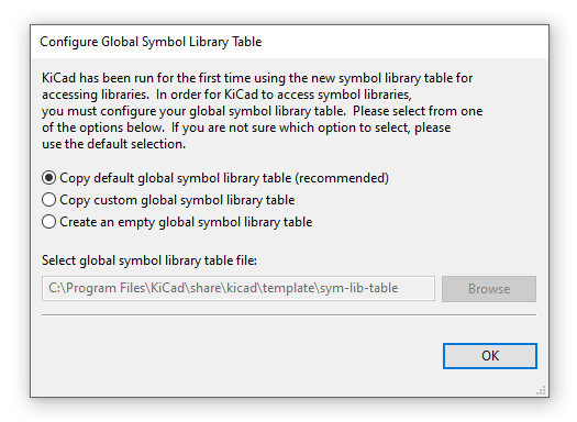
choco install kicadConfiguring The Global Symbol Library Table
Schematics
Getting Around
By default, the mouse wheel will zoom in/out on the current schematic.
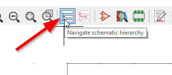
You can navigate the schematic hierarchy using the Navigate Schematic Hierarchy button as shown:
Keyboard Shortcuts
Mouse Wheel Zoom in/outMouse Wheel + Ctrl Pan left/rightMouse Wheel + Shift Pan up/downCtrl-D Load datasheet for selected component (opens web browser)The following keyboard shortcuts are to be pressed when the mouse cursor is over a component:
E Show symbol properties (Edit item).Ctrl-E Edit symbol (this loads up the symbol in the symbol editor).M Move schematic item.C Duplicate symbol or label.G Grab the end of a wire and shorten/lengthen it.A Place symbol (Add component).P Place power net.R Rotate item.Del Delete item.Shift-Enter Close a dialogue box (e.g. the edit symbol properties box)Importing Schematic Sheets
If you have an existing .Sch file you wish to add to your project, navigate to the parent schematic sheet you want to add the sheet to, and click Place->Hierarchical Sheet. Replace the contents in the file name box with the existing file, give it a logical sheet name and click o.k. KiCad will then prompt you saying “Filename already exists. Link sheet name to this file?”. Click yes and you’re done!
Schematic Page Templates
Click File->Page Settings to open the Page Settings window. You can select a template file for the Page layout description file field. The file must end in .kicad_wks.
Power Symbols
Unfortunately, power and ground symbols in KiCad are just standard library schematic symbols with the voltage baked into the part itself. This means you have to create a new library component if you want to have a rail with a voltage which isn’t in the default set of rail voltage symbols they provide with the installation! Ideally the voltage should just be considered part of the net name that is defined at schematic time, so you don’t have to keep creating library parts for custom voltage rails in your design!
The PWR_FLAG Symbol
The PWR_FLAG symbol is a special symbol in KiCad with one output power pin. This is typically attached to a power net which has no other output power pin attached (e.g. a connector pin which provides power to board, yet the pin is defined as electrically passive) so that the ERC knows that this net is provided power.
Libraries
.lib Schematic symbol library (contains multiple schematic symbols).pretty Folder for component footprintsBoth the schematic .lib files and the component symbol files are text based, so they play well with version control systems such as .git.
By default, the symbol libraries are installed to:
- On Windows:
C:\Program Files\KiCad\share\kicad\library - On Linux:
/usr/share/kicad/library/
Each project can pull schematic symbols and footprints from two “tables” (groups) of libraries, global libraries and project libraries.
DigiKey maintains the digikey-kicad-library, a KiCad schematic and footprint library of a large number of components that can be supplied by DigiKey. The aim of this library is to provide collection of visually consistent, accurate library parts that have been curated by the DigiKey team. The organization of the library follows the DigiKey family taxonomy.
Symbol Creation
The default grid step size is the symbol editor is 50mil (0.050” or 1.27mm). I recommend you leave the symbol grid size to it’s default when placing pins into symbols, as this will make the symbols consistent when placing onto schematics and prevent pins mis-aligning with the grid.
The KiCad symbol editor has a spreadsheet-style bulk pin editor window that lets you change the properties of multiple pins at once:

3D Models
3D models are stored at <kicad install dir>/modules/packages3d.
e.g. on Linux:
/usr/share/kicad/modules/packages3dThis directory is saved to the KiCad environment variable KISYS3DMOD. Inside this folder are folders named after part libraries with the suffix .3dshapes, e.g. Capacitor_SMD.3dshapes. Inside these folders are the 3D model .wrl files.
Unfortunately KiCad does not support relative file paths when linking 3D models to the footprints (relative to the footprint library). So you have two options:
- Use an absolute URL (which will work fine for one user but may break if more than one user will be using the library)
- Create a KiCad environment variable which points to the location of your 3D models (recommended approach)
Board Routing
Getting Around
Keyboard Shortcuts
D Start drawing a trackPgUp Switch to top layerPgDwn Switch to bottom layerF5 Switch to inner copper layer 1F6 Switch to inner copper layer 2+ Next copper layer (must already be on a copper layer for this to work)- Previous copper layer (must already be on a copper layer for this to work)Ctrl-B Hide poursB Show poursCtrl-H Toggle high contrast modeAlt-3 Load the 3D viewerSpace Reset the relative coordinate origin to 0,0 at the mouse cursorFor PCBs with up to 4 layers, you can use the PgUp, PgDwn, F5, F6 shortcuts to switch between copper layers. However once you exceed 4 layers you will have to use the + and -. It might suit you to just use + and - for any sized board, as there is less muscle memory needed!
KiCad has a push and shove router.
DRC Rules
As of May 2020, there is no way to add a check for silkscreen over pad in the design rules. The best you can do is select exclude pads from silkscreen when exporting the gerbers, which will remove all silkscreen from pads. This is not as ideal though, as this may remove important information from the silkscreen such as designators, version numbers or polarization marks.
PCB Layers
- Dwgs.User: Dimensions are placed on this layer by default
Generating Manufacturing Outputs
- Gerbers
- Drill files
- 3D model
File Types
.dcm # Schematic symbol library file. Stores the description, datasheet and keyword fields..lib # Schematic symbol library file. Stores everything about a symbol except the description, datasheet and keyword fields.-cache.lib-rescue.lib # Rescued library file.pro # KiCad project file.sch # Schematic sheet file.sch-bak # Backup of a schematic file.sym-lib-tablefp-info-cache # A cache file with info about footprints. This file is rebuilt often by KiCad..kicad_wks # A schematic page template file. These can be used in the File->Page Settings window within EEschema.KiCad expects the PCB filename to have the same basename (i.e. excluding the .pcb) as the project file (.pro). This has to be true if you want to open the PCB from the KiCad application by pressing the PCB Layout Editor button.
Output File Types
.gbr # Gerber plot file.drl # Drill file. KiCad fill name the files xxx-PTH.drl and xxx-NPTH.drl-drl.report # A drill report file, in a human-readable format-PTH-drl_map.ps # Drill file in PostScript format-NPTH-drl_map.ps # Drill file in PostScript formatPlugins And Python Scripting
On Linux, KiCad uses the system-installed Python (whatever the command python points to). On all other platforms, KiCad ships with it’s own version of Python.
On non-Linux platforms, you can find the Python executable at:
<KiCad installation dir>/bin/python.exe
e.g. on Windows:C:\Program Files\KiCad\bin\python.exe
Plugins are installed to:
<KiCad installation dir>\share\kicad\scripting\pluginsThe Windows version of KiCad ships with Python v2.7. If you want to use Python v3.x instead, you can rename python.exe located at C:\Program Files\KiCad\bin\python.exe to something like python.exe.old. This will cause the system Python to be invoked instead of the version shipped with KiCad. The big limitation with this technique is that none of the scripts will be able to import pcbnew, so it only really suitable for running scripts which do not depend on the Python KiCad API.
The KiCad C++ source code documentation can be found at https://docs.kicad-pcb.org/doxygen/index.html (generated by Doxygen).
Renaming A KiCad Project
In earlier versions of KiCad, it was unnecessarily difficult to rename a KiCad project. However, when attempted in KiCad v5.1.6 it is now possible! To do so, you will want to rename the following files all at the same time (updating the <ProjectName> bit), and from outside KiCad (make sure KiCad is closed when you do this):
<ProjectName>.pro<ProjectName>.sch: This is the “root level” schematic sheet. You don’t to rename other schematic sheets, just the one at the top-level in the hierarchy.<ProjectName>.sch-bak<ProjectName>.kicad_pcb<ProjectName>.kicad_pcb-bak
Once you have renamed all those files, you should be able to open this project in KiCad, your schematic/PCB links should work, and it will not complain about the changes!
Common Errors
Access Violation - Unable to create STEP file
This error can occur when generating a STEP file from within pcbnew. The error will look something like this:
Warning: Exception code=0xc0000005 flags=0x0 at 0x0000000066E952DA. Access violation - attempting to write data at address 0x0000000000000020Error: Unable to create STEP file. Check that the board has a valid outline and models.This can occur if you have “dangling” (to borrow C pointer terminology) links to 3D models which don’t exist. These should hopefully be printed as warnings before this error message, e.g.:
Warning: 10:58:21: C:/Jenkins/workspace/windows-kicad-msys2-stable/src/kicad/utils/kicad2step/pcb/oce_utils.cpp: AddComponent: 588Warning: * no model defined for component 'F201'Removing/fixing up these dangling 3D model links may remove the access violation error and allow you to create the STEP file. However I have encountered times when this fix alone does not remove the error, and are yet unsure of what to do next!
Simulation
The KiCad schematic editor (EESchema) supports mixed-signal SPICE simulation using the ngspice SPICE engine. Unfortunately, the simulation feature of KiCad is not very well documented. Your best bet is to start with one of the working examples provided by KiCad, and learn from there (see below). ngspice is bundled with KiCad so you do not need to download it separetly.
For general information on SPICE simulation, also see the SPICE Simulation page.
KiCad comes with example simulation circuits located at <KiCad installation dir>/share/kicad/demos/simulation/. In this directory there is the following simulation schematic example directories:
- laser_driver: Good example if you want to know how to include op-amps and transistors into your simulation. Notice that the pinout for the op-amp used in this schematic is very different to that of the op-amps in KiCAD’s two built-in simulation component libraries.

- rectifier
- pspice
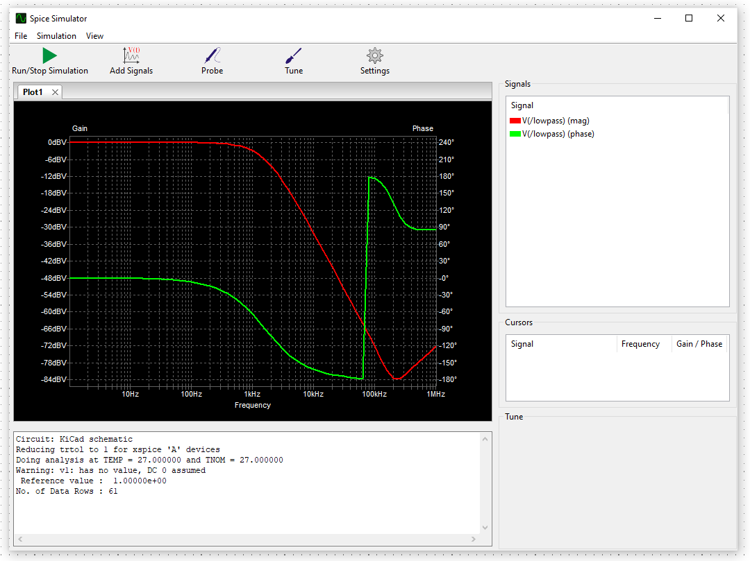
- sallen_key: Another example using op-amps, this time setup to perform AC analysis (i.e. produce gain and phase plots). Simulates a Sallen-Key low-pass filter.

Simulation Specific Symbol Parameters
There are a few schematic symbol parameters which have dedicated purposes for SPICE simulations. I’ve tried to list as many as I’ve encountered below:
Fieldname: TypicallyValue, pointing to theValuesymbol property. Think of this as a symbol property pointer?Spice_Primitive: This determines the element type (ngspice nomenclature)Rfor resistors,Cfor capacitors,Dfor diodes,Xfor subcircuits (anything that is built out of many primitives, i.e. ICs), e.t.c. See the below table for a list of all the supported primitives.Spice_Model: Only needed whenSpice_Primitive = X.Spice_Lib_File: Filename (not full path) of SPICE library component that belongs to this symbol, e.g.ad8051.lib. ClickingEdit Spice Modelshould bring up a dialogue box with the text from the.libfile.- The path can be either relative or absolute. If relative, it can be relative to the same directory as the
.schfile containing the component. Use forward-slashes in the path as these work on all major platforms (even Windows).
- The path can be either relative or absolute. If relative, it can be relative to the same directory as the
Spice_Netlist_Enabled: A boolean. eitherYorN.Spice_Node_Sequence: This is used to map KiCAD pin numbering with the pin numbering that ngspice expects. The value for this parameter is a space separated list of integers which map the KiCad pins to the ngspice pins. For example, almost all diodes in KiCad number the cathode as pin 1, and the anode as pin 2. ngspice expects things the other way around, with the anode as pin 1, cathode as pin 2. So simulation diodes should have aSpice_Node_Sequence=2 1.SpiceMapping:
The following table lists all the supported KiCad SPICE primitive types (what ngspice calls the element type) as of KiCad v5.1.6:
| First letter | Element description |
|---|---|
| A | XSPICE code model |
| B | Behavioral (arbitrary) source |
| C | Capacitor |
| D | Diode |
| E | Voltage-controlled voltage source (VCVS) |
| F | Current-controlled current source (CCCs) |
| G | Voltage-controlled current source (VCCS) |
| H | Current-controlled voltage source (CCVS) |
| I | Current source |
| J | Junction field effect transistor (JFET) |
| K | Coupled (Mutual) Inductors |
| L | Inductor |
| M | Metal oxide field effect transistor (MOSFET) |
| N | Numerical device for GSS |
| O | Lossy transmission line |
| P | Coupled multiconductor line (CPL) |
| Q | Bipolar junction transistor (BJT) |
| R | Resistor |
| S | Switch (voltage-controlled) |
| T | Lossless transmission line |
| U | Uniformly distributed RC line |
| V | Voltage source |
| W | Switch (current-controlled) |
| X | Subcircuit |
| Y | Single lossy transmission line (TXL) |
| Z | Metal semiconductor field effect transistor (MESFET) |
Voltage And Current Sources
Refer to the ngspice User Manual for a complete list of voltage and current sources. Voltage sources have their Spice_Primitive set to V and current sources to I.
These are called independent sources.
DC
For a simple DC voltage source, you can use the syntax:
DC VOLT
e.g. DC 5 for a +5V voltage source.
AC
Use the syntax:
AC <VOLTAGE>You may get the error Warning: vX: has no value, DC 0 assumed when running a simulation with an AC source which has no DC set point provided. This is generally o.k., as it will assume the DC operating point is 0V which is normally what you want.
If you are going to run an AC analsysis (i.e. using the .ac command), you don’t generally want more than one AC source in your schematic. If you have more than 1 AC source, the AC analysis results will be a superposition of all AC voltage sources and will be hard to interpret.
SINE
SINE(0 1.5 1k 0 0 0 0)
PULSE
The PULSE voltage/current source can be used to create a single square pulse or continuous PWM signal. The syntax is:
PULSE(VL VH TD TR TF PW PER PHASE)| Name | Parameter | Default Value | Units |
|---|---|---|---|
| V1 | Initial value | - | V, A |
| V2 | Pulsed value | - | V, A |
| TD | Delay time | 0.0 | sec |
| TR | Rise time | TSTEP | sec |
| TF | Fall time | TSTEP | sec |
| PW | Pulse width | TSTOP | sec |
| PER | Period | TSTOP | sec |
| PHASE | Phase | 0.0 | degrees |
For example, for a continuous pulse train alternating between 0 and 5V at 100kHz with a 50% duty cycle, with 10ns rise and fall times:
PULSE(0 5 0 10n 10n 5u 10u)Components
Resistors
To simulate say, a 10k resistor, start with any two pin symbol (using a resistor symbol would make sense, but that is not a requirement, you could use a two-pin smily face emoji if you want :-D) and make the following changes to it’s symbol properties (adding new properties where they don’t already exist):
| Name | Value |
|---|---|
| Value | 10k |
| Spice_Primitive | R |
Change the Value field for different resistances, e.g.
600(600 Ohms)2M(2 megaOhms)
Note that KiCAD automatically converts the commonly used M for megaOhms into the SPICE compatible meg (you may use meg directly if you want). Adding the symbol property with Name=Fieldname and Value=Value is not needed, this seems to be ignored, and KiCad will always use the Value property as the resistance. The symbol property SpiceMapping is also not needed, this seems like an older version of Spice_Node_Sequence and we do not need to adjust the pin mapping for a resistor anyway.
Capacitors
Follow the Resistor example above but use the following Value and Spice_Primitive values:
| Name | Value |
|---|---|
| Value | 100n |
| Spice_Primitive | C |
Inductors
Follow the Resistor example above but use the following Value and Spice_Primitive values:
| Name | Value |
|---|---|
| Value | 10m |
| Spice_Primitive | L |
Zener Diodes
To simulate a basic Zener diode, start with the D_Zener KiCAD symbol, and make the following changes to it’s symbol properties (adding new properties where they don’t already exist):
| Name | Value |
|---|---|
| Spice_Primitive | D |
| Spice_Model | D_Zener |
| Spice_Netlist_Enabled | Y |
| Spice_Node_Sequence | 2 1 |
| === |
Then add the following text to the schematic:
.model D_Zener D bv=5.0OR add another symbol property called Spice_Lib_File and add the path to a .lib file containing the same line as you would of added to a text field above. Spice_Lib_File can be either absolute or relative to a library root path.
Change the value 5.0 to whatever the blocking voltage of your Zener is.
Click here to download source files for a simulation that includes a Zener diode.
BJTs
The default pin ordering for BJT SPICE models is:
- Collector
- Base
- Emitter
However, KiCad’s default pin ordering for it’s BJT symbols is:
- Emitter
- Base
- Collector
The best way to fix this is to set the Alternate node sequence option to a value of 3 2 1.
MOSFETs
For discrete MOSFETs, the recommended approach is to use the VDMOS intrinsic model. This uses a standard 3-pin MOSFET symbol in the following order:
- Pin 1: Drain
- Pin 2: Gate
- Pin 3: Source
Make sure the symbol reference starts with an M, e.g. M1. Make sure the Value parameter contains the model name(e.g. 2N7002), and then add a line of text to the schematic containing the model parameters, e.g.:
.model 2N7002 VDMOS(Rg=3 Vto=1.6 Rd=0 Rs=.75 Rb=.14 Kp=.17 mtriode=1.25 Cgdmax=80p Cgdmin=12p Cgs=50p Cjo=50p Is=.04p ksubthres=.1)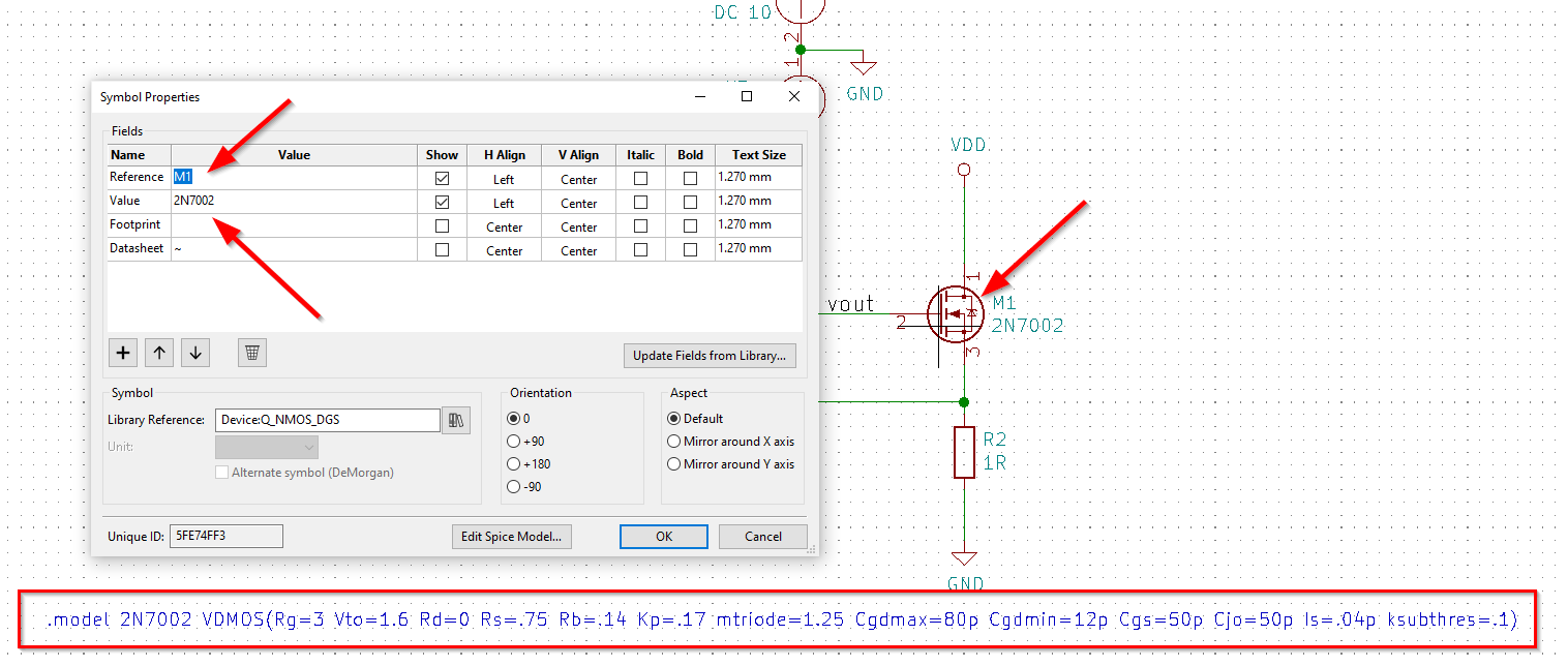
See the section 11.3 Power MOSFET model (VDMOS) in the ngspice User Manual for more information.
For MOSFETs built into integrated circuits, use the BSIM3 model. For the BSIM3 model, ngspice expects four pins rather than the usual three, gate, drain, source and bulk (substrate). In standard 3-pin MOSFETs the bulk is typically connected internally to the source, so for most simulations you can just do that externally to mimic a standard MOSFET.
See https://forum.kicad.info/t/generic-mosfets-solved/11155/3.
Looking for VDMOS intrinsic models? LTspice ships with over a 1000 of them. Once you install LTspice, you can find all the models within a single text file at LTspice<version>/lib/cmp/standard.mos. For example, on Windows with LTspice XVII the full path would be:
C:\Program Files\LTC\LTspiceXVII\lib\cmp\standard.mosMultiple Part Components
KiCad can properly convert it’s multiple part symbols (e.g. a op-amp IC with many op-amps, or a hex inverter IC) into a signal “component” when creating netlists for ngspice.
Custom Model Files
ngspice model files typically have the .lib extension --- the same extension as used by KiCad symbol libraries. Thus it’s easy to get these two confused, and makes it harder to search for system installed ngspice model files in the KiCad installation directory.
Placing Components
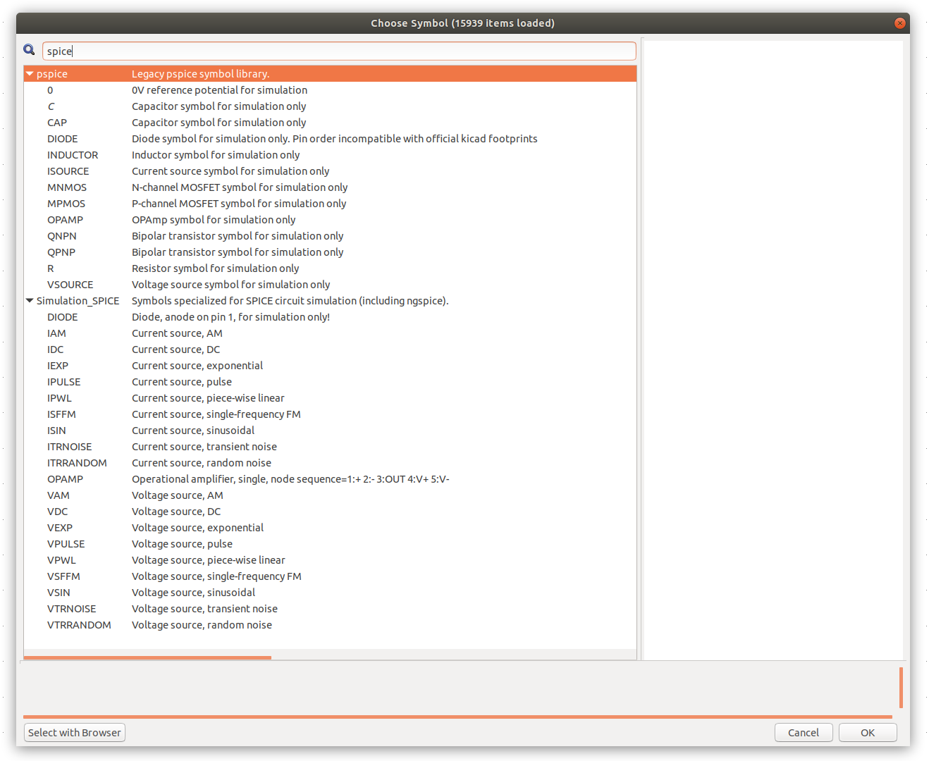
Somewhat confusingly, KiCad comes with two SPICE symbol libraries:
pspice: “Legacy pspice symbol library.” --- Presumably symbols which were used when KiCad used PSPICE.Simulation_SPICE: “Symbols specialized for SPICE circuit simulation (including ngspice).” --- Presumably newer symbols designed to work with the current bundled SPICE simulatorngspice.
Naming Nets
Standard Eeschema net labels can be used to name nets which will be carried through to the ngspice simulation.
KiCad will append a / to the front of all manually added net labels. This can be a pain if you were planning on using KiCad to just generate a SPICE netlist and running ngspice yourself, as you have to escape all net labels with the / by enclosing them in quotes (ngspice interprets / as the division operator). KiCad will not append a / for global net labels, so I recommend using those instead if you plan on running ngspice yourself.
Another way of dealing with this is to set the ngbehavior=ki (there is built-in functionality to ngspice to deal with KiCad output):
set ngbehavior=kiModes Of Analysis
There are three main modes of analysis:
- DC analysis: The time varying behaviour of reactive elements is ignored.
- Basic DC analysis: Analysis of the circuit with each voltage/current source at a single DC level.
- Swept DC analysis: Basic DC analysis but repeated at a number of different DC input levels for the voltage/current sources.
- AC analysis: The simulator outputs magnitude and phase information as a function of frequency. Good for analyzing passive and op-amp based analogue filters.
- Transient analysis: The entire circuit, including DC and reactive elements is simulated. The output is the voltage and currents at each node as a function of time.
Although KiCad allows you to configure modes of analysis through the simulation GUI window, this information is not saved with the schematic and gets lost every time you restart. I recommend you add a text string on the schematic instead.
Transient (.tran)
Transient analysis simulates the behaviour of the circuit through time.
Syntax: .tran tstep tstop <tstart <tmax>>
e.g.
.tran 1u 10mtstart is optional. If no tstart is provided, tstart is assumed to be 0. Note that the transient analysis always begins at t=0, tstart specifies the time at which to begin recording data. This is useful if you want to let the circuit reach a steady-state before recording data.
DC Sweep (.dc)
The DC sweep analysis mode (.dc) has many different forms and supports many different types of analysis.
Syntax: “
To do a basic sweep of voltage source V1 (which must exist in your schematic with designator V1) from 0V to 5.0V in increments of 0.1V:
.dc V1 0.0 5.0 0.1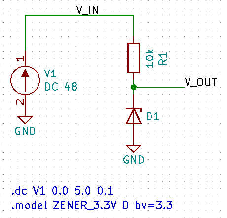
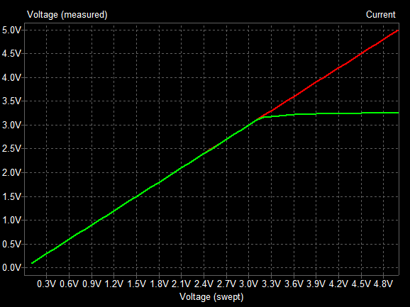
Click here to download the source files for this simulation example.
AC Analysis (.ac)
Syntax:
.ac dec nd fstart fstop.ac oct no fstart fstop.ac lin np fstart fstopFor example, to simulate the response of the circuit from 1Hz to 10MHz:
.ac dec 10 1 10MegIf you are going to run an AC analysis (i.e. using the .ac command), you don’t generally want more than one AC source in your schematic. If you have more than 1 AC source, the AC analysis results will be a superposition of all AC voltage sources and will be hard to interpret. To quote the ngspice manual:
Note that in order for this analysis to be meaningful, at least one independent source must have been specified with an ac value. Typically it does not make much sense to specify more than one ac source. If you do, the result will be a superposition of all sources and difficult to interpret.
Printing Out The Version Of ngspice
You can print out the version of ngspice by adding the following text to the schematic:
.controlversion.endcngspice will then print out the following information when the simulation is run:

Saving Plots
You can save the data on the plots through the GUI. Click File->Save as .csv file. The CSV file will be semi-colon delimited. Rather than outputting a header row with the names of the columns of data and then each successive row being a data point, the csv file will contain a row (new line) for each axis
Note that is frequency is plotted on the x-axis, KiCad/ngspice will incorrectly export the data as Time in the csv file.
Common Simulation Errors
unknown subckt
I have got the following error when the wrong Spice_Primitive was set (the component was a diode, Spice_Primitive was set to X for sub-circuit, was meant to be set to D).
Error: unknown subckt: xd1 <net name> 0 1n5817Error: there aren't any circuits loaded.There are duplicate components. You need to annotate schematics first.
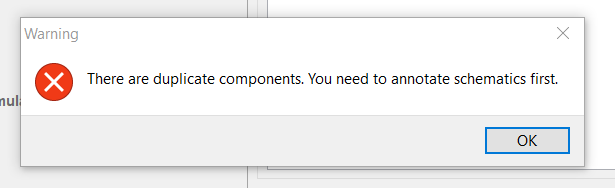
This error usually arises if you have not assigned unique designators to all components. Perhaps there are still R?, C? e.t.c designators on the schematic? Or multiple instances of properly labelled components, such as two R1’s. The best way to fix this is just to reset and re-annotate the schematics.
You need to select the simulation settings first
This error pops up if ngspice cannot find a mode of analysis directive. Rather than choosing the simulation settings, I recommend you enter the directive in as text on the schematic instead.
See the Modes of Analysis section for more info.
doAnalyses: iteration limit reached
doAnalyses: iteration limit reachedrun simulation(s) aborteddoAnalyses: Timestep too small
doAnalyses: TRAN: Timestep too small; time = 1.75691e-08, timestep = 1.25e-23: trouble with node "xu2.xay.60"run simulation(s) abortedThis error can occur during the time stepping of a transient analysis. SPICE has an internal timestep which keeps changing, if voltages/currents are changing slowly then SPICE keeps the timestep large, if voltages/currents are changing rapidly then SPICE reduces the timestep. This error occurs if SPICE keeps reducing the timestep and keeps failing to converge. As some point it hits a lower limit (which is typically orders of magnitude lower than the timestep you specified) and the simulation bails.
CICD
The GitHub user productize has created some Python scripts in the GitHub repo kicad-automation-scripts which automate some core KiCad processes such as running ERC (electrical rules check on the schematics) and DRC (design rules check on the PCB). Along with committing the KiCad design files to version control systems such as Git, these tools can be used to implement CICD workflows that run automatically on changes/commits.
Handy KiCad Plugins
InteractiveHtmlBom
Website: https://github.com/openscopeproject/InteractiveHtmlBom
This plugin shows you a render of the PCB alongside the BOM and lets you select component lines on the BOM, which highlights all the components on the PCB. It’s a great tool to use when hand assembling prototype PCBs.