Altium Tricks And Standards
After using Altium for many years, you begin to pick up on little tricks to make your PCB design life easier. This page is intended to help you fast-track that!
It pays to have some basic standards/protocols when working with Altium, otherwise things can get ugly real quick.
Schematic Symbol Snap
Rule: Keep schematic snap when designing symbols to DXP defaults.
This is because most schematic symbol libraries use this setting, and if you don’t, using other peoples symbols don’t connect properly. I recommend you use a snap that is a multiple of 5mill. This only applies when placing the pins, you can choose whatever you want for the rest of the symbol! I regularly use 1mill snap for designing graphics for the symbol.
If you don’t get the snap right, it is really hard to connect pins up on the schematic, and Altium will produce “Component off grid” warnings when compiling. An overload of these can mask any true mistake where a component is not connected to the intended net.
One PCB Per PcbDoc And PcbPrj File
Altium was designed so that there is only one PCB per .PcbDoc file. And it was designed so that there is only one .PcbDoc file per .PcbPrj file. A single PCB is defined as one continuous board region.
Problems with having multiple PCBs per .PcbDoc:
- Altium only supports a board outline which outlines a single continuous region. To add multiple PCBs, you have to add a joining link of board between the two actual PCBs, which looks ugly in both 2D and 3D modes.
- All the nets have to be unique between the two PCBs. This becomes a problem for commonly used names such as 5V and GND. If you don’t have unique names, Altium will want you to join the two PCBs together with copper, thinking you have an unrouted net.
- Designators have to be unique across the two PCBs. This means that designators on one of the PCBs won’t start from R1, C1, e.t.c.
Folder Structure
Create a different folder for each project - With all the files Altium creates for a project, directories can get really, really messy.
Stopping Rooms From Being Added To The PCB
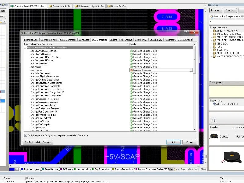
Also, rooms can get annoying when you don’t need them. To disable rooms, click Project → Project Options → ECO Generation. Select Add Rooms and then choose Ignore Differences from the drop-down menu on the right. Delete any existing rooms, and Altium will no longer automatically add them when you update the PCB.
My Vias/Tracks disappear When I’m Routing!
This is caused by Altium’s Automatically Remove Loops function removing vias and tracks when you have more than one connected to the same trace. To stop this from happening, begin routing, and then press TAB. The routing options windows will pop up. Navigate to the Interactive Routing Options section and deselect Automatically Remove Loops.
Version Control Systems
If you are using Mercurial source control software for you Altium project, here is a recommended Mercurial Ignore File to prevent the un-necessary files from being put under version control.
The Board Shape
Altium allows close integration between the mechanical and electrical design with the ability to define the board shape from DXF/DWG files or step models. I personally find the DXF format perfect for defining the board shape from a mechanical design, in where you can create a board-outline DXF by exporting from CAD software such as SolidWorks or GeoMagic.
PCB Layer Standards
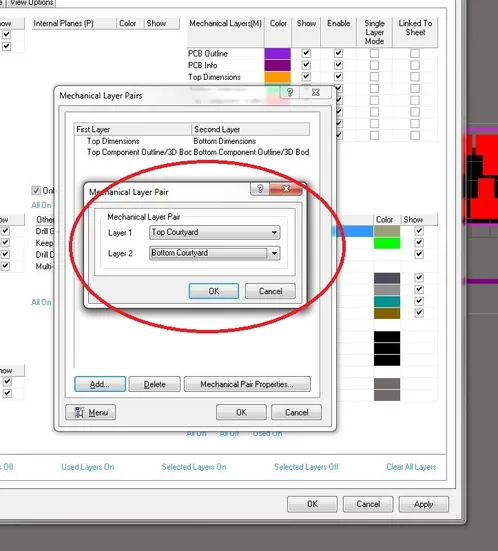
These conform to the default layers that Altium’s IPC Footprint Wizard automatically uses for certain parts of a component. Some of the layers are paired, so that Altium automatically switches the objects on these layers when the component is changed from top layer to bottom layer and vise versa.
| Layer | Usage |
|---|---|
| Mechanical 1 (M1) | Board outline (it is not recommended to use just the keep-out layer, since that can be used for other things also). |
| Mechanical 2 (M2) | PCB notes and comments for the PCB manufacturer/assembler (included in Gerber output). |
| Mechanical 3 (M3) | General notes and comments that the PCB manufacturer/assembler does not need to know about (not included in Gerber output). |
| Mechanical 11 (M11) | Top layer dimensions (paired with M12). |
| Mechanical 12 (M12) | Bottom layer dimensions (paired with M11). |
| Mechanical 13 (M13) | Top layer component body information (3D models and mechanical outlines, paired with M14). |
| Mechanical 14 (M14) | Bottom layer component body information (3D models and mechanical outlines, paired with M13). |
| Mechanical 15 (M15) | Top layer courtyard and assembly information (paired with M16). This normally includes a cross-hairs at the origin of the component. |
| Mechanical 16 (M16) | Bottom layer courtyard and assembly information (paired with M15). This normally includes a cross-hairs at the origin of the component. |
The pairing of the mechanical layers is done as shown below.
Layer Colours
I find that when using many Altium layers, the default colour scheme can get very confusing. To make things simple to understand, I like using a ‘hot and cold’ colour scheme.
All layers related to the top side (Top Layer, Top Overlay, Top Paste, Top Solder, Top Dimensions, Top Component Outlines/3D Bodies, and Top Courtyard are all chosen to be hot colours, while conversely all the bottom side layers are chosen to be cold colours.
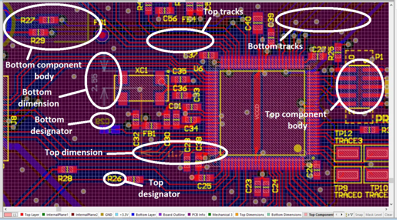
The file [TransparentHotColdPcbViewConfig v1.0.config_2dsimple](/docs/TransparentHotColdPcbViewConfig v1.0.config_2dsimple) and loaded into Altium to setup the colour scheme as mentioned above.
PCB Symbol Naming Convention
A good idea is to follow Altium’s PCB symbol naming convention, which can be downloaded from the Altium website here.
Component Description Standards
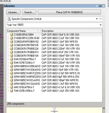
The component description is commonly used to convey all the important parameters of the component that that are vital for the BOM. For example, the description of a capacitor might indicate that it’s a capacitor, the type of capacitor, the package size, the temperature coefficient, tolerance, voltage and capacitance in a short hand notation.
The idea is that the “Description” field will be added to the BOM, and it will be solely responsible for describing the part to whatever detail is necessary.
It is useful to use the component description for this purpose to make the BOM easy to understand and use. Because each type of component has its own unique set of parameters, If all these values where included in their own separate parameter fields, the BOM would become large, full of empty fields (e.g. a resistor typically does not have a temperature coefficient) and unnecessarily messy.
I use the following notation for the description field. The parameters are listed in short-hand from most generic to least generic (this allows for good grouping when sorting alphanumerically). The symbol reference is set the manufacturer’s part number, as this has to be a unique field.
Capacitor Labelling
Below is a good way to label Capacitors:
Capacitor, <type>, <package size (imperial)>, <capacitance>, <voltage>, <temperature coefficient>, <tolerance>e.g.
Capacitor, Ceramic, 0603, 10nF, 35V, X7R, 5%Resistor Labelling
Below is a good way to label Resistors:
Resistor, <package size (imperial)>, <resistance>, <tolerance>, <rated power>e.g.
Resistor, 0402, 2.70k, 1%, 63mWQuickly Adding Vias To Nets
To quickly associate a via to a net, when placing the via, make sure to place it over a track or pad with the same net. The via automatically inherits the connected net.
Getting To Datasheets Quickly
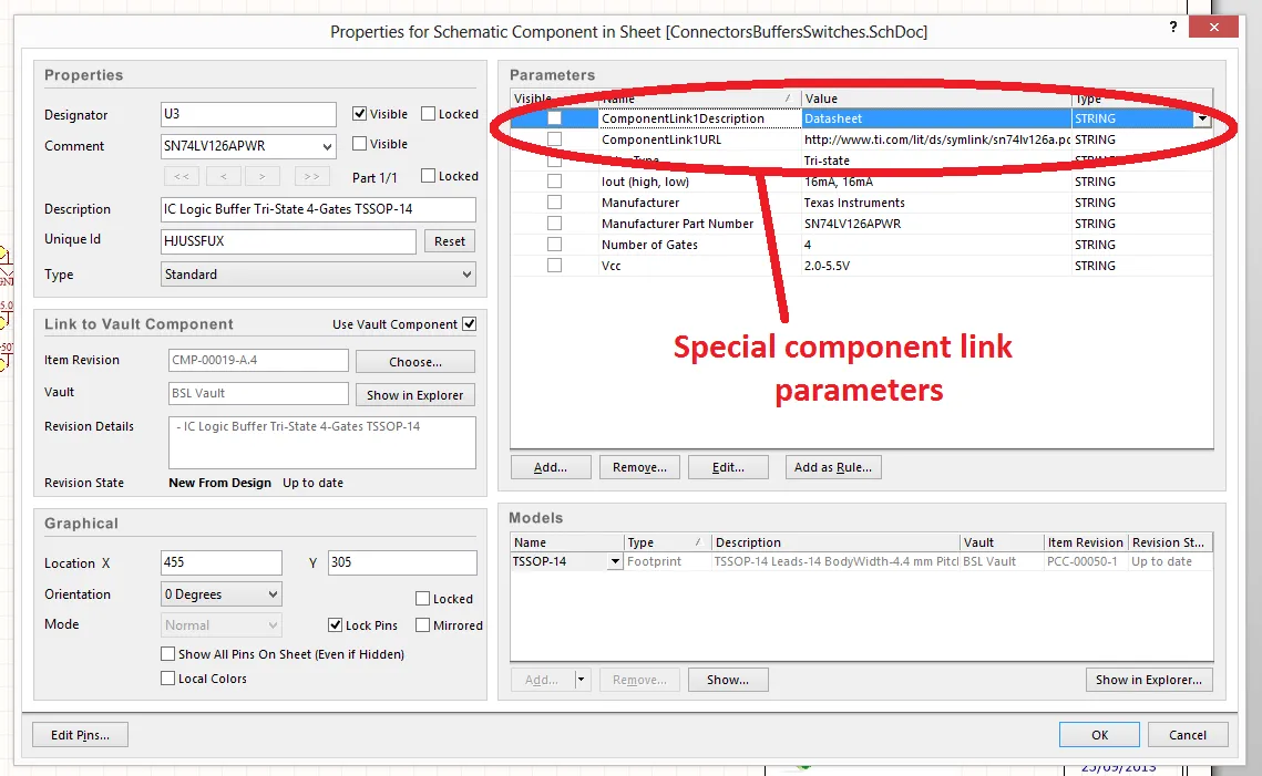
Over and over during the PCB design process you’ll find yourself wanting to go to the datasheet of a component you can see on a schematic. There is a quick way to add a link to the right-click context menu of the component in Altium by adding a component parameter that follows a special syntax.
These special component parameters are called component links, and follow the syntax:
| Parameter Name | Parameter Value |
|---|---|
| ComponentLink1Description | Enter the name you want to see in the right-click menu |
| ComponentLink1URL | Enter the URL you want to go to when you click. |
| ComponentLink2Description | Enter the name you want to see in the right-click menu |
| ComponentLink2URL | Enter the URL you want to go to when you click. |
| … | … |
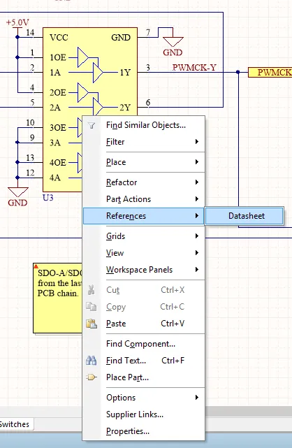
This can be repeated for as many component links as you wish. The URL can be any valid path (i.e. the path to a file on your computer/server, or to a website URL). They can be added to both schematic library component parameters, and component library parameters which will the be released to a vault. The component links get added to the References sub-menu when you right-click on the component in the Altium schematic editor.
For example, I would add these component parameters to a buffer IC:
| Parameter Name | Parameter Value |
|---|---|
| ComponentLink1Description | Datasheet |
| ComponentLink1URL | http://www.ti.com/lit/ds/symlink/sn74lv126a.pdf |
As shown in the following image:
I would then be able to quickly go to the datasheet by right-clicking the component, navigating to the “References” sub-menu, and clicking “Datasheet”.
Using Transparent Layers
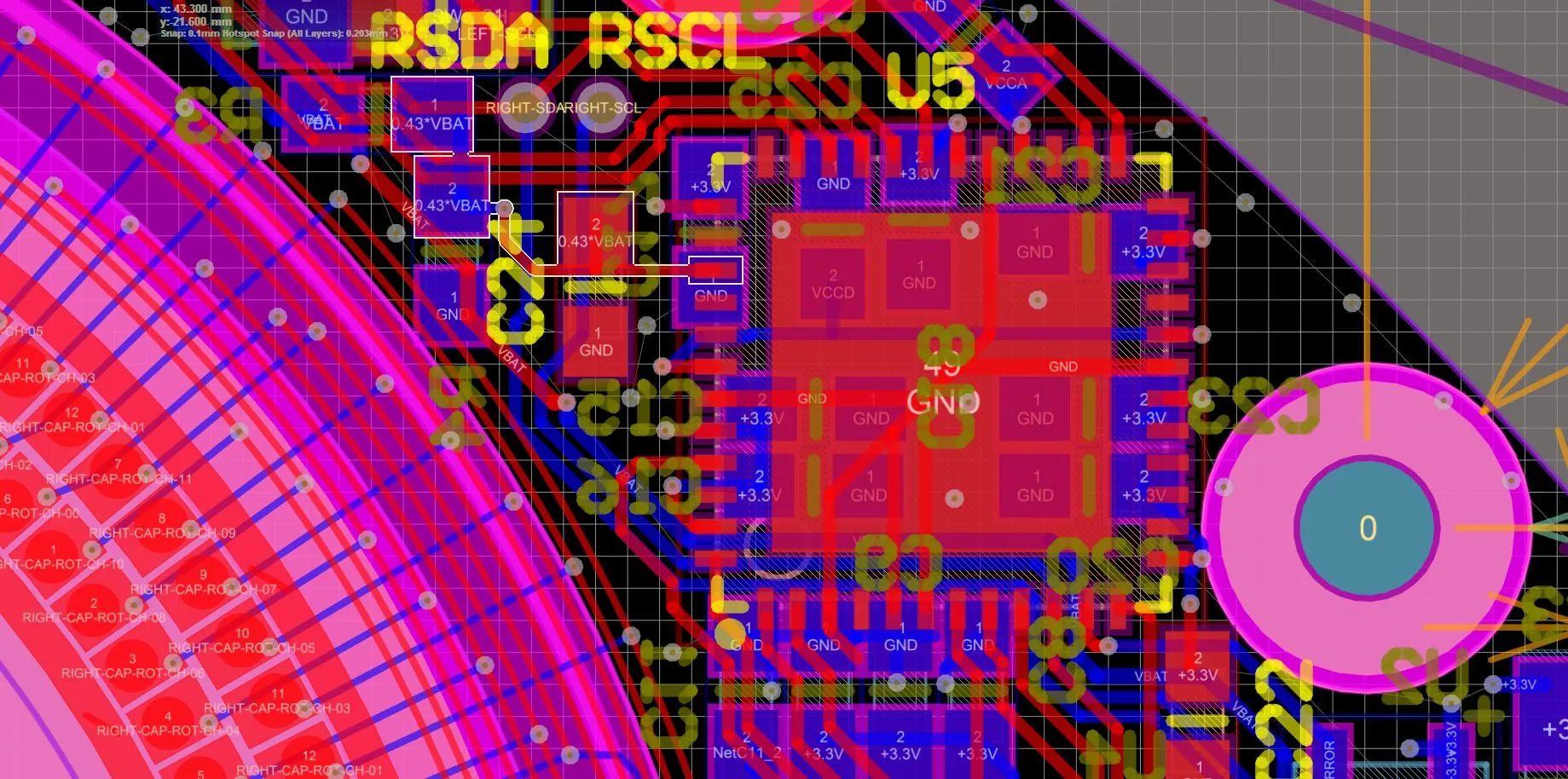
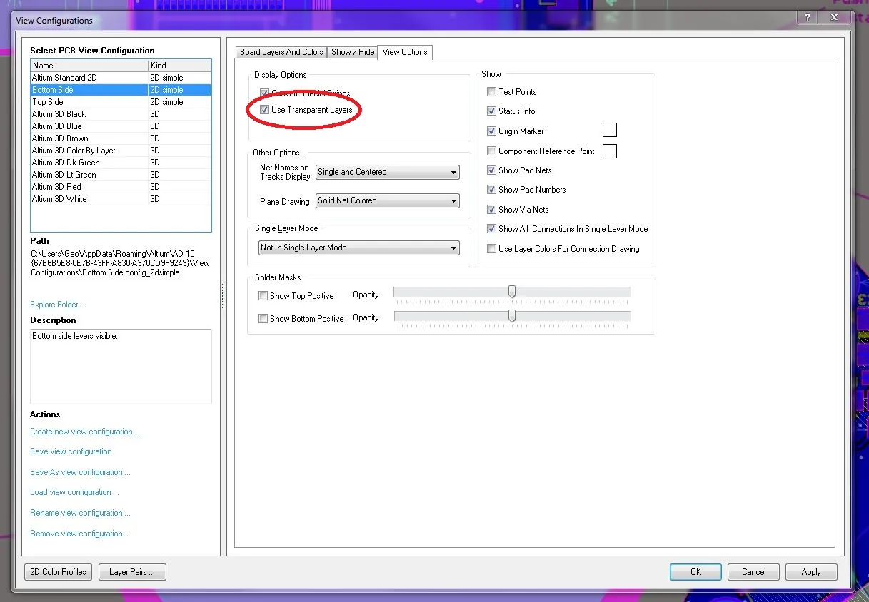
‘Use Transparent Layers’ is a menu option hidden away in Altium that makes the layers go semi-transparent. It is really useful when dealing/routing with multi-layer objects (such as vias). I found I use Transparent mode more often than not now since I discovered it. To enable it, go into the View Configurations Menu, click the ‘View Options’ tab, and then make sure the ‘Use Transparent Layers’ box is ticked as shown below.
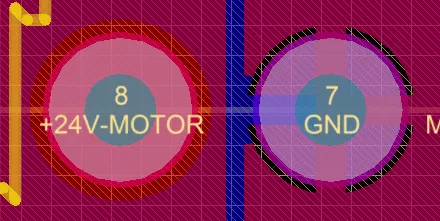
Here is an example showing layers when set to Transparent mode.
Direct Connect For Specific Pads
When designing a PCB, you often find yourself wanting to “direct connect” from polygon pours and power planes to specific pads of a component, while leaving the others with thermal relief connections. This is usually to reduce the copper track resistance to high current pins (e.g. V+ and GND).
The simplest way to do this is to add a custom pad region around the pin of interest. However, this is time consuming as you have to do it for every pin and on every layer. A better way is to use pad classes.
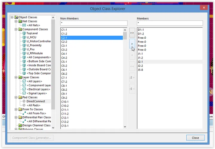
To add pads to a pad class, first take note of the component the pad is part of in the Altium PCB editor, and the pin number of the pad itself (e.g. component J3, pin number 2). Now click Design->Classes. Navigate the folder “Pad Classes”, and add a new pad class called DirectConnect (the exact name does not matter). Now add all the desired pads to this new pad class.
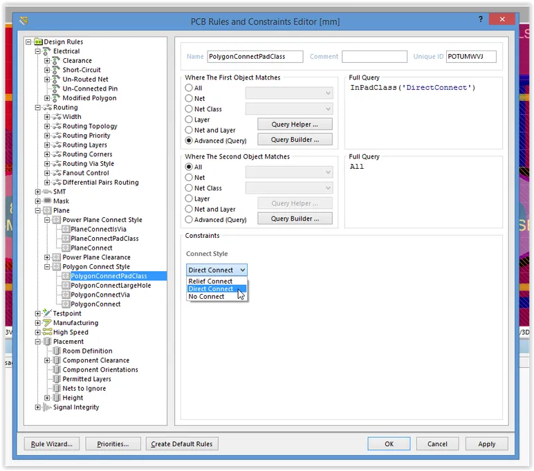
We now need to make a direct connect rule for all pads in this pad class. Click close, and now click Design->Rules. Add a new “Polygon Connect Style” rule. Select “Advanced (Query)” for the first object match, and then enter InPadClass(‘DirectConnect’) into the “Full Query” window. Change the Connect Style to “Direct Connect”.
Save and exit the Rules dialogue, and rebuild your polygons. Done! You should now have direct connects to all the pads you added to the “DirectConnect” pad class. If you want to do the same thing for power planes, add a similar “Power Plane Connect Style” rule for the same pad class, as shown in the above picture. If you want to add pads to class which don’t belong to any component, look for them under “Free-xx” (e.g. Free-0) in the pad classes dialogue.
If all the pads that you are wanting to direct connect are located in the same area, you may want to use a PCB “room” object to envelop all the pads instead of adding each pad to a pad class. Another disadvantage of the pad class trick is that this direct connection information will be lost if you change the designator (or worse still, will be assigned to completely wrong pads who just happen to have the same name as the old ones).
Opening Internet Links In External Web Browser
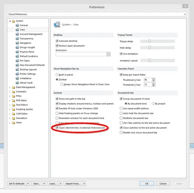
By default, Altium tries to open internet links in it’s own internal browser. It’s no surprise that because Altium is a EDA tool and not a dedicated browser, it’s not the best at displaying web pages. Thankfully, you can force Altium to use your default external web browser by navigating to DXP->Preferences->System->View and checking the “Open internet links in external Web browser” option.
Removing Exposed-Pad Vias That Are Automatically Added By The Footprint Wizard
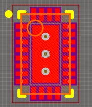
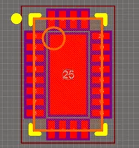
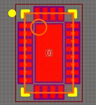
The Altium footprint wizard automatically adds vias to the exposed pad of component package footprints such as QFN. Although it is recommended to have thermal vias conducting heat away from the exposed pad to the other PCB layers, it causes problems when these vias are added to the footprint, because of the inflexibility to change them during the PCB design stage. Without unlocking the primitives of the footprint (which I do not recommend you do unless absolutely needed), there is no way to modify these vias during the PCB design. You may wish to move them to allow for nets to pass underneath the component footprint on another layer, you may wish to add more for better thermal properties, or you may wish to remove them altogether because it recommends for that specific chip to leave the thermal pad unconnected.
For these reasons, I recommend that you delete these automatically added vias from all affected component footprints, and instead add vias as needed during the PCB routing stage of the design process.


