Altium Bugs And Things To Watch Out For
There’s no denying Altium has it’s quirks. If you are getting annoyed with one of Altium’s bugs, submit it to BugCrunch, their bug tracking and fixing sub-site (you can vote on what you want fixed first). Here a some of the things you should keep an eye out for…
Custom Soldermask Expansions
Custom soldermask expansions added to tracks on a PCB file won’t carry across when you go and panelize (an embedded board array) it. They way to get around this (albeit slightly annoying) is to use polygon’s instead of tracks, the soldermask expansions carry across for these.
Please Wait A Moment
Applicable Versions: 14, 15, 16
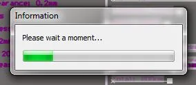
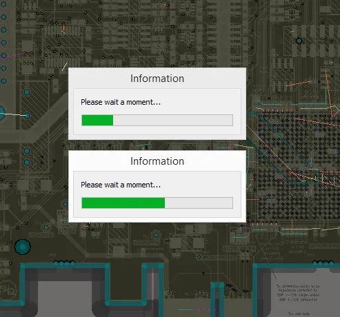
Altium crashing with a ‘Information’ title box that says ‘Please wait a moment’, and a forever scrolling progress bar. At the point, save as much work as possible (you can still operate some commands at this point), and quit.
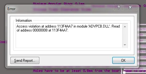
The error you sometimes get after the “Please Wait A Moment” box.
UPDATE: As of Altium v14.0, running on a Windows 8 machine, I have noticed far fewer of these errors!
Closing Altium When It Crashes
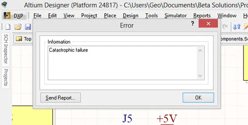
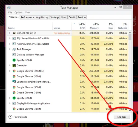
The easiest way to close Altium when it crashes it to hit Ctrl-Alt-Delete, bring up the task manager, go to the processes tab, and close DXP.exe. This is plenty faster than closing the program Altium.exe from the same task manager (almost instant, rather than 30+ seconds).
”Argument out of range” Errors
Applicable Versions: Altium 16
Last Updated: April 2016
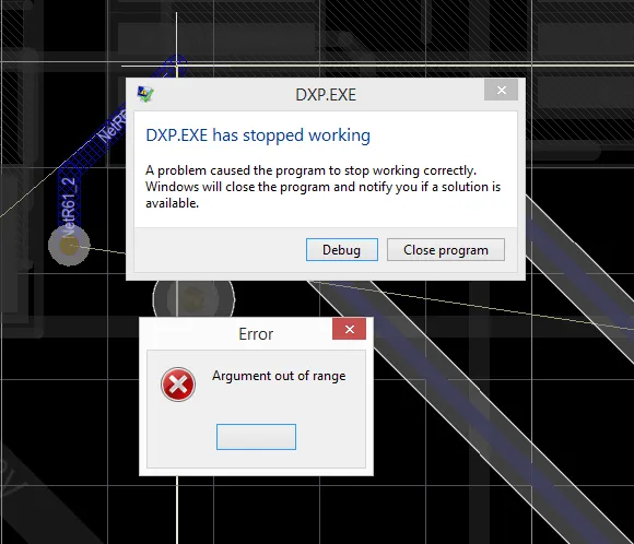
I have got fatal “Argument out of range” errors while performing basic routing tasks on the PCB. There is no way to save any work when this occurs, and after clicking the “O.K.” button of the many “Argument out or range” boxes that pop-up (which are glitchy), Altium crashes and closes automatically.
Vias Disappearing While Routing Tracks
UPDATE, March 2016: This does seem to occur anymore with at least either AD15 or AD16.
Vias disappearing when you route tracks to them. This is a weird one which has been around for a while. It only happens in certain situations…
Almost Full-Circle Arcs Disappearing At Certain Zoom Levels On Schematics
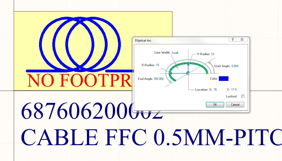
If you draw an arc with the intention of drawing a full-circle but don’t close it completely, you may notice that it will disappear at certain zoom levels (or just disappear entirely). This seems to happen when the start and end angle of the arc are very closer together (for example start angle = 0, end angle = 359.9). A way to fix is to edit the properties of the arc and make the start and angle the same.
Copy/Pasting Images Into Altium
You can put images into Altium schematics, but don’t do it via the copy-paste way from a program that has an unsaved image (like Snip). In my experience, this causes Altium to crash with the infamous “Please Wait A Moment…” message.
Holes/Vias In Step Files
UPDATE, March 2016: This does not seem to be happening anymore with AD15 or AD15.
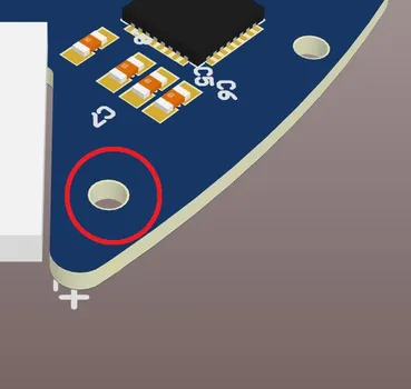
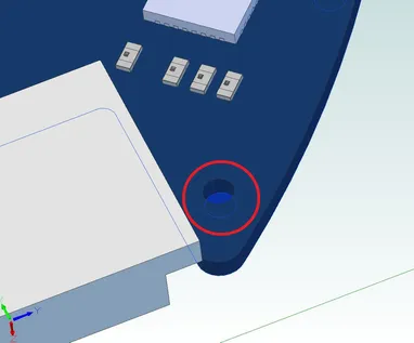
Altium decides whether or not it wants to export holes/vias in step files. Upon importing these step files into a 3D CAD program, more often than not you will find that some of the holes have been covered (or partially covered) up by a very thin solid on the top and/or bottom. I have tried removing copper, silkscreen, soldermask and solderpaste layers to see if these were causing the trouble, but have had no luck in finding out why Altium does this. It is very annoying when it doesn’t create the mounting holes, and you can’t check that the PCB will work with the rest of the mechanical design (which is normally one of the reasons why you’d be exporting a 3D model).
Variants With Multi-part Components
Multi-part components do not work well with schematic and PCB ‘variants’. The multi-part components do not become ‘not fitted’, even when selected to do so, and will still appear on both the BOM and 3D views of the PCB.
Removing Soldermask From Pads
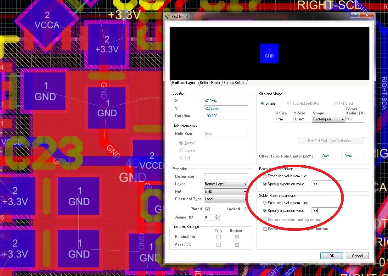
To remove soldermask/solder paste from pads, the only way to do it is to go into the pads properties (double-click it), and then change the “Soldermask Expansions” (or Paste Mask…) option from “Expansion value from rules” to “Specify expansion value”. Then you have to set it to a negative value large enough the it will shrink it away to nothing (e.g. larger than than the radius of the hole/via itself). I normally just enter -99mm or something along those lines…
Searching Altium Libraries
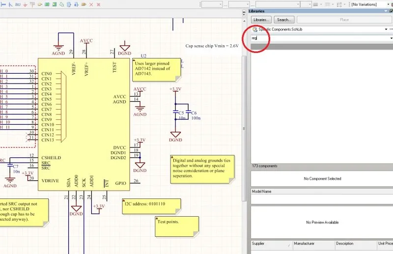
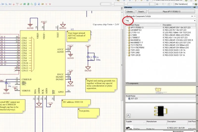
When searching through a library, Altium will only search from the first letter of the component name or the description. This normally makes you search turn up blank. To make Altium search anywhere in those fields, add the asterisk character before the word (e.g. *reg rather than reg).
Timestamping Output Files
Timestamping output files is a good idea of keeping track of releases intended for pcb manufacturer’s/assemblers (as well as version numbers). Timestamping can be added to the automatic file generation by selecting the option under the advanced tab of the “Output Container” properties window. However, Altium follows your system clock format when creating this timestamp, so it will likely be in a dd-mm-yyyy or mm-dd-yyyy format, which when sorted alphanumerically, does not sort in chronological order. To fix this, change your system time to the yyyy-mm-dd format.
Scripting Will Remove The Ability To Undo
Using scripts to add objects to a PCB can remove the ability to undo in any PCB during the current Altium session. This may have something to do with not calling specific undo functions from the script after the object has been added and it getting confused from that point onwards…
Polygon Clearance Rule Not Working
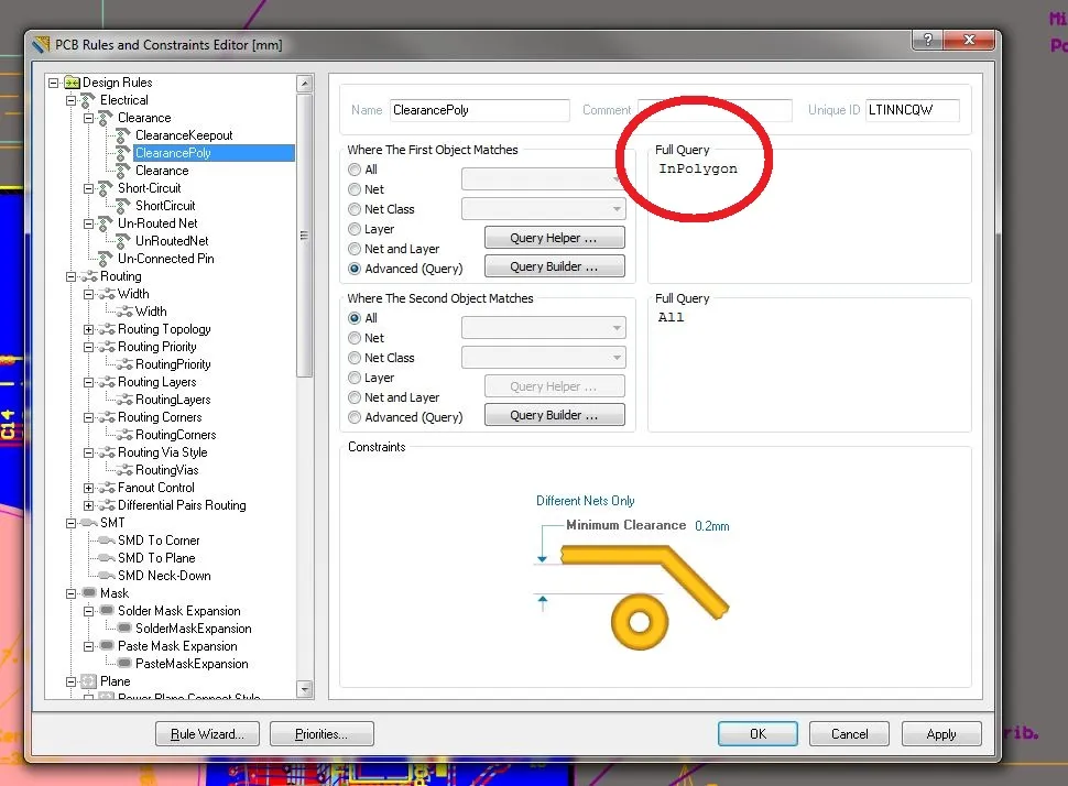
When setting the clearance rule in Altium. make sure that when you set the ‘First Object Matches’ query, you use the term ‘InPolygon’ rather than ‘IsPolygon’. This is because Altium treats all the copper which you wish to apply the clearance rule to in the polygon as an object which is ‘in’ the polygon object. See the example in the picture below.
Clearance Rules On The Keep-out Layer Are Not Working Properly With Polygons
If you are finding that when you draw polygons that Altium is not staying the correct distance away from zones you draw on the keep-out layer, you are probably caught by one of Altium’s ‘gotchas’. When deciding the clearance between a track on the keep-out layer and any polygon (or any other object for that matter), it calculated from the EDGE of the track, not the centre. When you think about it, this makes sense, since this is the behaviour you would expect if drawing solid objects on the keep-out layer as fills. However, it can be quite annoying when using tracks.
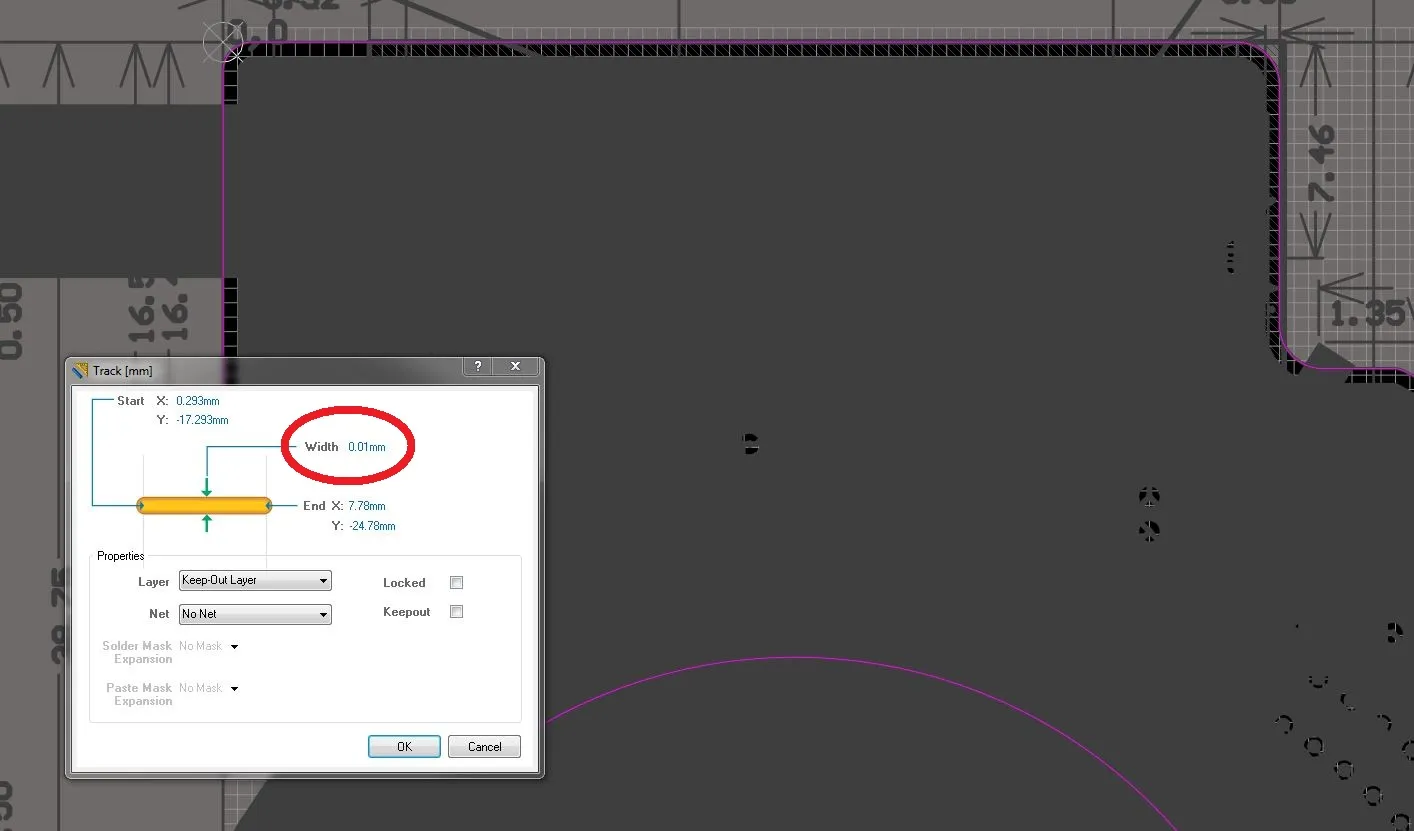
What I do to workaround this is to make the width of any tracks on the keep-out layer small in relation to the clearance you need (e.g. track width = 0.01mm). This way, the track width makes an insignificant change to the actual clearance. The picture below shows part of a PCB board along with thin-width tracks on the keep-out layer to set clearances properly. Note that the keep-out layer clearance is set to 0.5mm (a good value to keep things away from the edge of the board), while the track width is only 0.01mm resulting in an actual clearance of 0.5005mm (clearance + half the track width).
Altium And It’s Geometrical Limitations
Altium works with straight lines and circular arcs. There is no provision for higher-order shapes such as polynomials or splines. A let-down is that rooms cannot be defined with arc segments, only lines. The board shape can be defined from both (by using the “Define board from selected primitives” option.
Printing Scaled Altium Documents
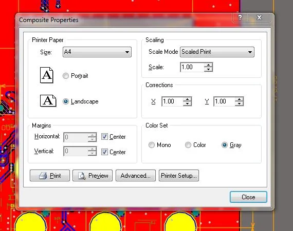
In my experience, a ‘scaled’ Altium Document printed on a standard laser printer has a decent amount of measurement error, and cannot be relied on for things such a mechanical checking or PCB prints and defintely not for etching. This is likely not to be a bug in Altium but the printer’s fault (well, even then, it’s not really the printers fault, a standard laser was probably never designed to be able to print accurate drawings).
Altium Detecting Acute Angles Inside Pads
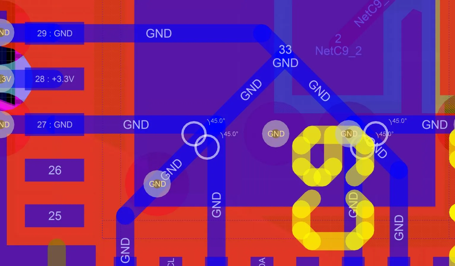
Altium will give you warnings about acute angles when the tracks are inside pads (and therefore don’t actually get drawn). This normally occurs in the central pad of SMD IC packages (such as QFN). The solution to this finish tracks just as they enter pads rather then letting them snap to the centre of the pad. To do this, hold down CTRL while routing the track, this will stop it from snapping to the centre.
Layer Stack-Up Manager Calculating Wrong Height
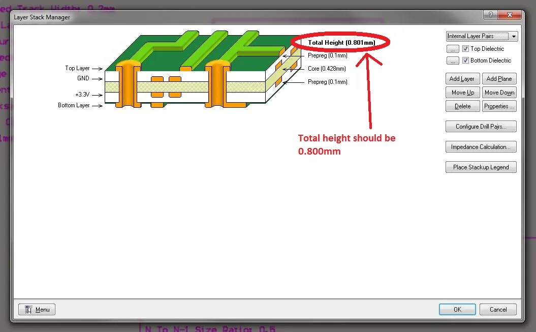
The layer stack manager seems to incorrectly calculate the stack-up height by 1um (O.K., it’s not that important, but still…). See the screen shot below for an example. All the copper thicknesses are 35um. It should total to 0.800mm, but Altium incorrectly reports it as 0.8001mm.
Combo Boxes In Script Form Forgetting Their Items
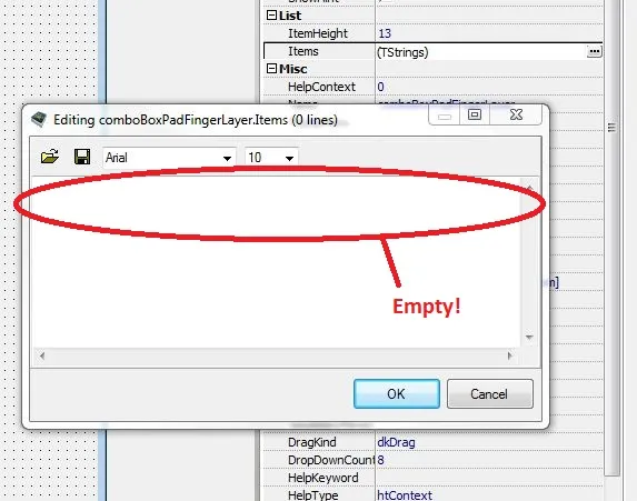
The combo boxes in the script form designer forget their items if you set them using the GUI, save, and then restart. The way to get around this is to add the items at run time in the code itself (using the function comboBox.AddItem).
Screen Artifacts
Every so often small screen artifacts can appear. These are defintely one of the more tolerable Altium bugs. To fix, usually you have restart Altium, as refreshing the window or minimising/maximising does not remove them. The artifacts are usually sections of the ‘Projects’ menu on the left-hand side of the screen.
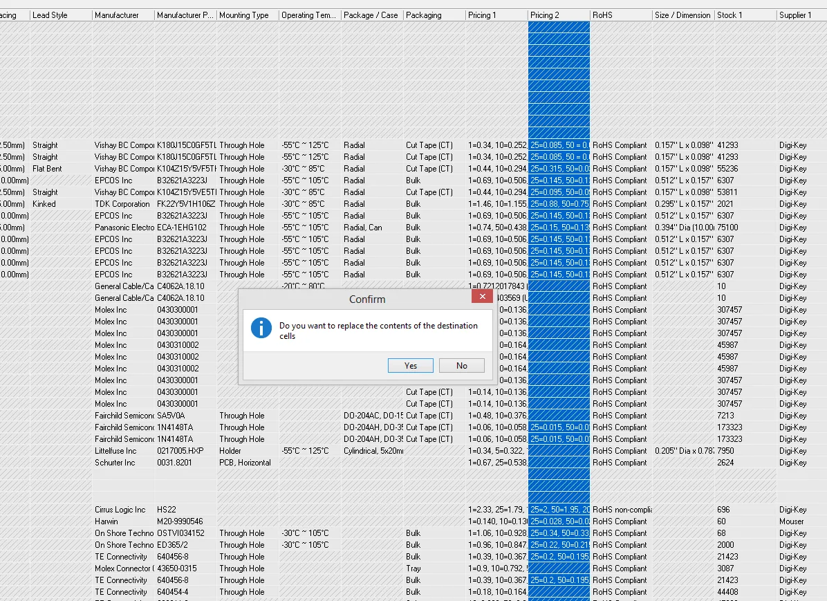
Clearing Cells In Parameter Manger Takes Ages
When clearing a large number of cells (>20) in the Parameter Manager , Altium can take plenty of time, stalling the program in the process (it looks as though Altium has locked up).
Undo/Redo Issues When Editing Component Primitives On PCB
When you unlock component primitives on a PCB and start editing them (say you want to edit the silkscreen of a component just for a specific PCB, and not edit the component library), you can get into weird problems in where the undo/redo functions will not work properly.
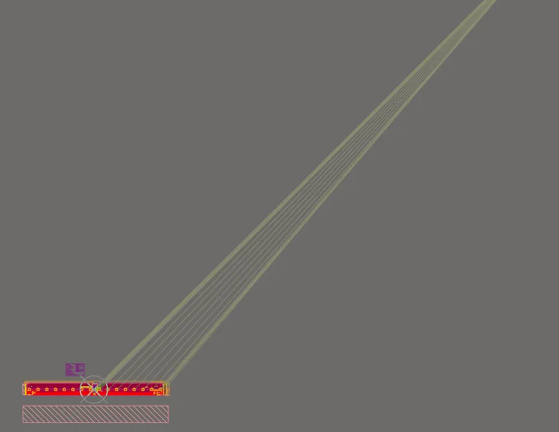
PCB Objects Going Out Side Of The Editor Boundary
When creating PCB footprints in Altium’s PCB editor, you can sometimes accidentally places things outside of the editors boundary. This can happen for example by accidentally typing the wrong number in the Move by X, Y command, a buggy script, or hitting copy/paste at the wrong time.
Once this occurs, it can be ridiculously hard to delete this objects, because they cannot be selected (even with Select->Outside Rectangle). These objects then appear during the PCB design (you may not even realise they are there) at times when you want to zoom to fit, or creating PCB print outputs (in which everything will be zoomed out by way to much to accommodate these far-away objects).
Schematic Parameters Un-removable After Script Modifications
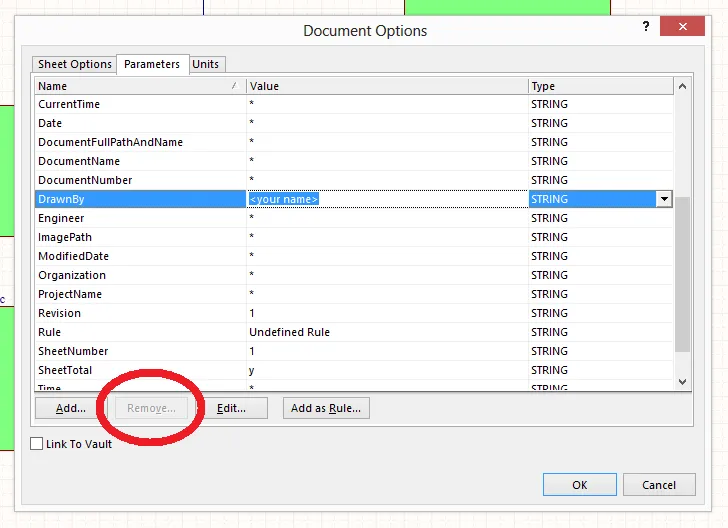
In certain cases, I have noticed that the schematic preferences become un-removable after they have been modified with a script.
No Multi-line PCB Strings
UPDATE, 2015-11: The Altium PCB editor now supports multi-line strings. Hurrah!
Altium does not have support for multi-line PCB strings. The work around is build up your multiline PCB string from many single line strings. This is time consuming, annoying, and seems like a waste of time.
Split-planes Don’t Avoid On-Layer Keep-Out Objects
The split-planes which Altium pours automatically do not ignore on-layer (i.e. on the split-plane layer itself) primitives which have been defined as “keepout” (e.g. a keepout region). This isn’t such a bad thing, as knowing that it is a split-plane, you can just make the primitive non-keepout, and since split-planes are negative, it will avoid this object.
Issues With Vaults
I have used the personal vault and come across the following issues:
There Is No Option To Set Default Parameters
Remember when using schematic libraries (.SchLib), and you were able to set “shown-by-default” component parameters which would be visible when using the component on a schematic? Well, they no longer exist (as of Jan 2014), and there is no option in the component libraries (.CmpLib) to make any of those parameter you add shown by default. This means you have to manually go and make them visible for every component you add from the vault (e.g. resistance for resistors, capacitance and voltage for capacitors). This gets kinda annoying!
In the same vein, if you update a shcematic component with a new version from the vault via the “Properties for Schematic Component…” window, you lose all of the displayed parameters and have to tick them all over again.
The Personal Vault Looses Track Of Who Is Logged In
In the scenario where more than 3 people may access the vault (not all at the same time), I have had Altium lock me out because it believed 3 other users were currently using it, even though Altium was shutdown on their computers. The only fix I have found is to restart the server that the vault is running on.
No Way To Re-arrange Groups In Component Libraries
There is no way to re-arrange “Groups” in Component Libraries (.CmpLib). You can re-arrange components by clicking and dragging, but the groups are stuck in the same position as when you first created them. This can be annoying in the instance say, you created a component library for resistors, and you had a group called 0402, 0603 and 0805. Unless you create them in the correct order at the start, there is no way to re-arrange them from smallest to largest size in the future.
Also, the first group you create is always going to be the first group (due to the fact you cannot insert a new group above an old one, only below)!
UPDATE (2014-11-04): As of Altium Vault 2.0 (released in 2014), this is no longer an issue, as the “Group” concept in the vaults has been changed significantly.
A Component Cannot Have Sub-Components
Frequently when designing more complex boards you come across the desire to be able to create a component which creates multi-entries on the BOM. This could be thought of as a component having many sub-components. For example, if you have a particular arrangement of 2.54mm pitch header connectors which allows you to plug-in, say an Arduino, it would be nice to be able to group these all-together as a single component (i.e. an Arduino connector), yet when it comes to BOM creation, you want to be able to list the individual headers for purchase.
This would also mean that the entire component could be dragged around on both the schematic and PCB without the sub-components movings relative to each other.
Unfortunately, I do not know any feasible way of doing this (yet)! If anyone has any ideas, please let me know…
Altium Does Not Support Co-Planar Waveguides
Altium provides support for impedance-driven routing. However, in only calculates desired track widths for microstrips and striplines, and not co-planar waveguides (with or without ground).
Keep-out Regions On Split-Plane Layers Do Not Work As Expected
Keep-out regions on split-plane layers do not stop the split plane copper from being drawn over them! You have to use actual copper pours, and since the split-plane layers work as a negative, this will prevent actual copper from being poured in these areas.
Hidden Pins On Schematics Can’t Be Attached To Visible Pins
On the surface, it seems like Altium gives you the option to hide pins on a schematic symbol and attach them to other, visible pins on the schematic symbol.
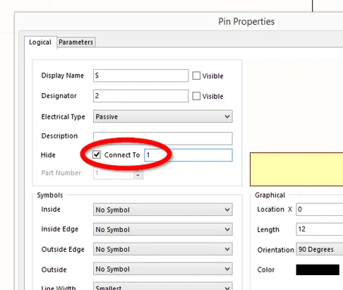
This would be very useful for certain component/package combinations which use multiple pins for the same purpose. Such an example are MOSFETs in the SOIC-8N component package. The standard pinout for connecting the three MOSFET terminals to the 8-pin SOIC-8N package is source = pins 1 to 3, gate = pin 4, drain = pins 5 to 8.
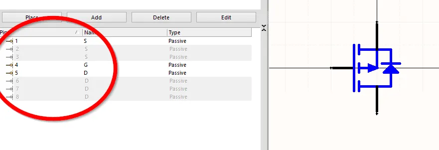
The only solution is to ditch the “hide” ability altogether and stack the pins ontop of each other. One downside to this approach is that Altium will show a multiple connection dot on the schematics when you wire up to pins stacked ontop of each other. But then again, maybe this is not such a bad thing?
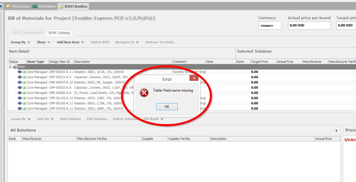
Table: Field name Missing Error On BOM Open
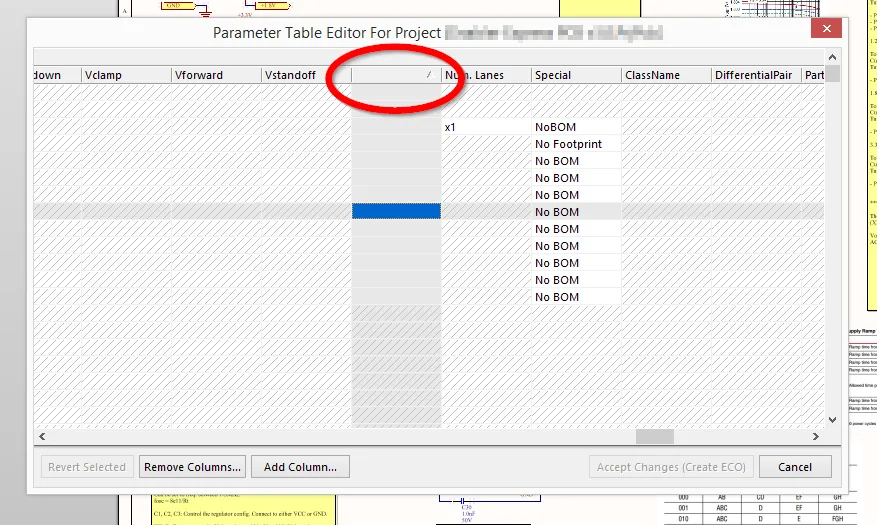
If you get the error “Table: Field name Missing” when opening, modifying, or saving a BOM (for me it occurs when using a .BomDoc), it is usually because your Altium project contains components which have parameters with no name.
Parameters are allowed to have no value, but not no name. To fix this, delete all unnamed parameter in your project. The easiest way to do this is to load up the Parameter Manager and hunt down for parameter names up at the top of every column that are blank, and then delete them.
PCB Editor Can’t Handle Unicode Characters In Component Descriptions
Unicode characters (which are not ASCII), such as the Ohm symbol and the degree symbol, while supported by the schematic editor, component libraries and vault system, are not supported by the PCB editor.
Because of this, the PCB editor will continuously try and update component descriptions which contain Unicode characters on every “Update Changes From Schematics” command.
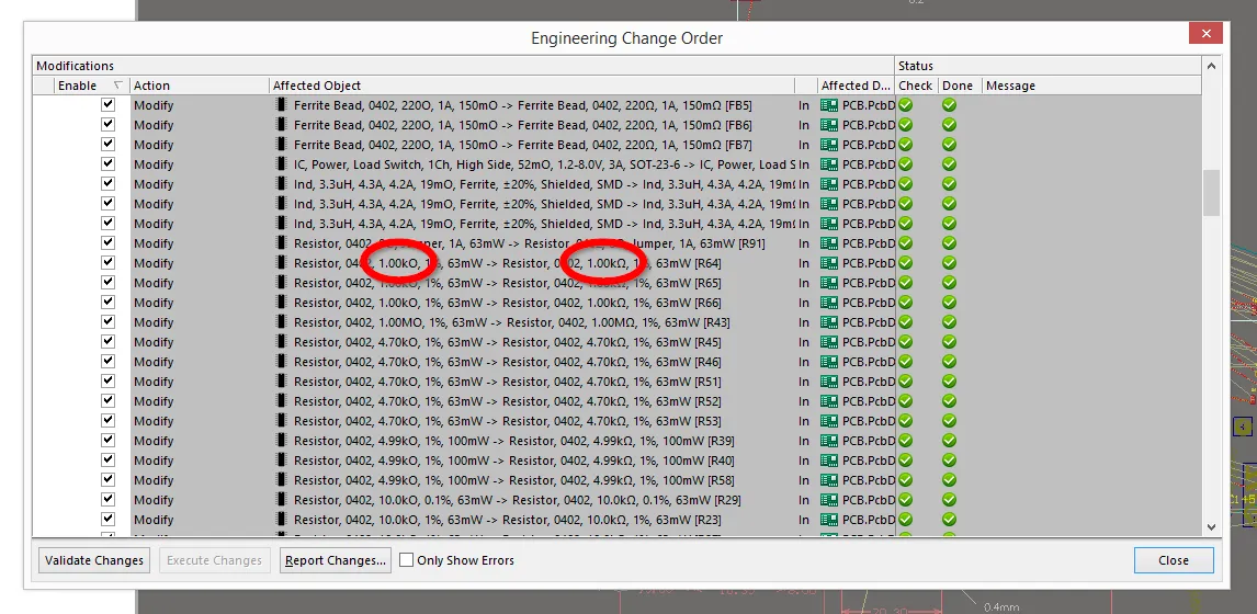
This is unfortunate, as symbols like and are great to use in component descriptions.
BomDoc Gets Modified When You Don’t Want It To
Affected Versions: AD15, AD16
The .BomDoc file allows you to define the supplier of each PCB component. It is compatible with the Component libraries and the vault system.
The problem is that the .BomDoc file decides to reload in live supplier data at inconvenient times. This file modifications can clutter file change history (when Altium is used within a version control system such as Git or Mercurial).


