Linear Regulators
Linear regulators are devices which vary their “resistance” to generate a fixed and stable output voltage (or sometimes output current). Excess voltage/current is dissipated in the linear regulator as heat, and for this reason they can get quite hot when the voltage difference between input and output is large, and/or the load requires high current. In these situations, a more efficient switch mode power supplies (which uses switching elements and energy storage in inductors/capacitors) may be more suitable.
Linear regulators are only capable of producing an output voltage which is lower than the output voltage. For regulators capable of producing higher output voltages, see switch mode power supplies or charge pumps.
Linear regulators are great when you want a cheap, low power voltage regulation solution. They can also be used on the output of a SMPS regulator (which are far noisier) to reduce the voltage ripple (the ripple will be reduced by the linear regulators high PSRR).
Topologies
There are two common topologies used for linear regulators (configurations):
. Series: The linear regulator is placed in series with the load. . Shunt: The linear regulator is placed in parallel with the load.
Series Linear Regulators
Series linear regulators work by comparing the output voltage to a accurate (and usually internal) voltage reference, and use the error to dynamically adjust the resistance of a series pass transistor (or other active element) by turning it more or less “on”. The transistor’s “resistance” drops the input voltage down to the required output voltage.
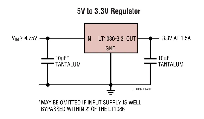
Series linear regulators are relatively simple components to connect up into a larger circuit, typically only requiring an input pin, output pin, and either a GND (for fixed voltage versions) or ADJ pin (for variable voltage versions):
Shunt Linear Regulators
Confusingly, shunt regulators are commonly shown in schematics as a zener diode with a third pin coming from the middle of the rectangle, as shown below. This zener diode symbol hides significant complexity, in reality they are actually a integrated circuit containing a voltage reference, op-amp and BJT!
One common use for these devices is a shunt voltage regulator, as shown below. The trick here is that will turn on as much as it can to make the voltage at its pin equal to it’s internal voltage reference (which is commonly 2.5V). By connecting up to the resistor divider and , you can get to shunt regulate to a chosen , as long as it’s above .
It is quite easy to show that the output voltage in the above circuit is calculated as given in Eq .
Min/Max Shunt Regulation Current
A shunt regulator will have a minimum and maximum current at which it is able to regulate correctly. For example, the LM431 has an of and a of .
Popular Shunt Regulators
LM431
| Property | Value |
|---|---|
| Part Number | LM431 |
| 2.5V | |
| 2.5-36V | |
| 1-100mA | |
| Package(s) | SOIC-8, SOT-23, TO-92 |
Popular in the feedback circuit of flyback converters.
Important Parameters
- Maximum current (A)
- Output voltage (or voltage range if adjustable, )
- Input voltage range
- Protection circuitry (current limit, input polarity reversal, thermal limit)
- Junction-to-ambient thermal resistance of linear reg package (, °C/W)
- Power-supply rejection ratio (, dB)
- Maximum operating temperature
Low Dropout Regulators
Low dropout regulators are a special sub-family of series linear regulators that have much smaller dropout voltages (typically , does depend on max. load current) compared with traditional linear regulators which have a typical dropout of . However, low dropout regulators tend to be more prone to oscillation and more strict about capacitance requirements on the input and output.
Thermal Considerations
The power lost as heat through a linear regulator is:
where:
is the output voltage
is the input voltage
is the current through the regulator.
The regulator has to be able to dissipate this power without exceeding the maximum operating temperature. The temperature that the linear regulator will operate at is given by:
where:
is the junction-to-ambient thermal resistance
is the ambient temperature
Protection
While you easily blow up regulators in the 1990’s, even the very cheap modern-day regulators have built in protection circuitry which makes them basically indestructable. Most feature excess current protection, thermal protection (most turning off above if their die temperature exceeds 150-170°C), short-circuit protection, reverse-polarity protection, and input disconnect (reverse current flow) protection. One of the only ways to kill them is over-voltage on either the input or output.
This is further compounded if you are using an adjustable linear regulator and have added a filter capacitor on the ADJ pin — the charge on the capacitor can flow back through the ADJ pin and cause problems. A second diode from the ADJ pin to fixes this problem:
Bypass Capacitor
Variable output-voltage linear regulators usually have a feedback pin for setting the voltage. This pin is normally connected to the centre of a resistor divider between the output pin and ground. The ratio of the resistances determines the output voltage. When using these types of linear regulators, it can help to have a bypass capacitor between the output pin and the feedback pin. These are also known as feedforward capacitors.
Adding capacitance here helps improve the AC characteristics of the linear regulator, which includes:
- Better transient response to load changes
- Increases the PSRR (power supply rejection ratio)
- Decreases the noise added to the line by the linear regulator
A typical value of a bypass capacitor is .
Power Supply Rejection Ratio (PSRR)
The power supply rejection ratio (PSRR) (a.k.a power supply ripple rejection, but the acronym stays the same) measures a linear regulators ability to block noise on the input from reaching the output. It is expressed as a logarithmic ratio in dB of the noise that appears on the output when noise is presented on the input.
Basic Equation
DDR Termination Regulators
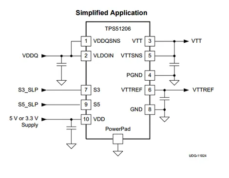
DDR termination regulators are special-purpose linear regulators designed for powering DDR memory ICs. They usually provide the multiple voltage rails that are required to drive DDR memory, along with the power control logic required to meet the DDR spec. (incl. suspend to RAM, suspend to disk states).

DDR memory draws current in quick surges of around 2-3A. Most DDR termination regulators support both the sinking and sourcing of current, which means they can clamp the voltage if an overshoot occurs due to a fast switching transient. Standard linear regulators cannot do this, and only source current.
Foldback Current Limiting
Foldback current limiting (a.k.a. voltage-dependent current limiting1) is when the short circuit current of a linear regulator is decreased to a value less than the max. current when the output is at it’s normal operating voltage. This is done to protect the series pass transistor in a linear regulator, as it can otherwise start dissipating too much power and overheat.
Foldback current limiting is usually done when simple current limiting is not effective, for example in high output voltage linear regulators which are rated to a high current. Under normal operation, the difference between input and output voltage is small and the power dissipation in the series pass transistor is also consequentially small. But if the output is shorted, now almost the full input voltage is dropped across the pass transistor, causing the power dissipation to shot up.
For example, a 15V in, 12V 1A out linear regulator under normal conditions would dissipate 3W of heat. In the event of a short circuit on the output, without foldback current limiting, this would increase to 15W! A foldback current circuit would maybe limit the short circuit current to 200mA, thus the same 3W is dissipated under the event of a short.
The below circuit shows how foldback current limiting is typically implemented in a linear regulator (either internally or externally to an IC):
The below graph shows the V/I response of a linear regulator with foldback current limiting. As the load resistance decreases, the output voltage stays steady at until is reached. Then both the output voltage and current reduces, with the current decreasing to as the load resistance reaches (direct short).
How Foldback Current Limiting Works
- Under normal conditions, is off and turns on enough to regulate the output voltage as normal.
- As the load current increases, the voltage drop across increases.
- When the load current reaches a certain point, the voltage across is large enough that when divided down by and , it reaches and begins to turn on .
- robs of base drive, turning it more off and thus reducing the output voltage.
Design Procedure
The maximum load current before foldback current limiting will kick in is given by the equation below:
where:
is the desired regulated output voltage under non-fault conditions, in Volts []
is the forward base-emitter voltage drop, approx.
All resistances as shown in [^foldback-current-limiting-circuit] in Ohms []
The short-circuit current when falls to is given by Eq. .
Example Devices
The TPS7A4001 is a high-voltage (100V) linear regulator which can provide up to 50mA of current.
The LM78xx series (for fixed positive voltages) and LM79xx series (for fixed negative voltages) of linear regulators have traditionally been very popular choices. They are not low dropout.
The LM317 (for adjustable positive voltages) and LM337 (for adjustable negative voltages) are also very common.
Footnotes
-
Simpson, C.. SNVA558: Linear and Switching Voltage Regulator Fundamentals. Texas Instruments. Retrieved 2021-08-31, from https://www.ti.com/lit/an/snva558/snva558.pdf ↩


