Op-Amps
At it’s most basic level, an operational amplifier (op-amp) is a discrete analogue integrated circuit which acts as a voltage-amplifier with very high gain.
An op-amp’s gain can be adjusted with the appropriate external circuitry (the op-amp’s internal gain does not change, but the gain of the entire circuit does). This is almost always done for any op-amp that is used as an amplifier. External circuitry can also manipulate the op-amp to act as as a current amplifier or perform “mathematical” operations on signals.
Schematic Symbol
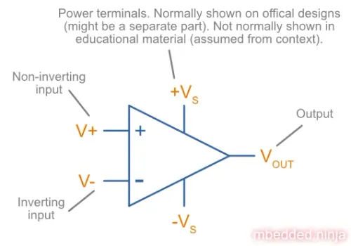
An op-amp is commonly drawn on schematics as:
You may see this symbol with or without the voltage supply pins and . If they are not present, it is assumed that they are connected up to a power source which should be obvious from the design intent.
Uses
- Buffers (a.k.a. voltage followers)
- Linear amplifiers, non-linear amplifiers
- Pre-amplifiers (amplifier’s with a input voltage of 10mV or less)
- Analogue mathematical operations (differentiators, integrators, summer, subtracters, e.t.c)
- Voltage to current (transconductance) and current to voltage conversions (transimpedance)
Op-Amp Topologies
Voltage Followers (a.k.a. Buffers)
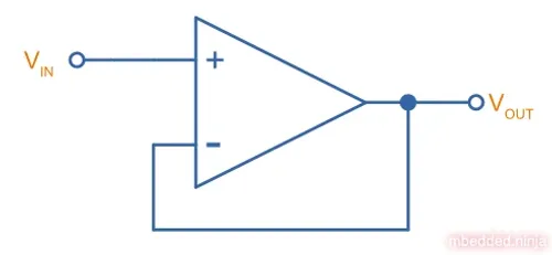
A voltage follower (also known as a buffer) is one of the most basic circuits you can make with an op-amp. The schematic is shown below:
The output voltage for a voltage follower is just simply:
As shown in Eq , the output voltage is the same as the input voltage. Well isn’t this pointless? No, the key point to a voltage follower/buffer is that it can convert a high-impedance input into a low impedance output. Practically, this means that you can now sink/source more current from the output without the voltage changing. Buffers are great for boosting signals that travel across long distances, or for signals which get split and go to many devices (this is called fan-out, and is common with digital clock signals).
Non-Inverting Amplifiers
A op-amp in the non-inverting amplifier configuration is shown below.
The equation for the output voltage of the non-inverting amplifier is:
Notice the in the gain equation? This means that no matter what you set the resistors and to, you can never get a gain which is less than one. This is one of the disadvantages of the non-inverting amplifier (you can have a gain of less than one with an inverting amplifier).
Inverting Amplifiers
A op-amp amplifier in the inverting configuration is shown below.
The equation for the output voltage of an inverting amplifier is:
The negative sign is to show that the output is the inverse polarity of the input. Notice that, unlike the non-inverting amplifier, an inverting amplifier lets you obtain a gain of less than 1.
Difference Amplifiers
A difference (a.k.a differential or subtractive) amplifier is an op-amp circuit which amplifies the voltage difference between two electrical signals. It is the mathematical equivalent of subtraction with some additional gain. The schematic is shown below:
The output voltage is given by the equation1:
To make a standard difference amplifier, is picked to equal and is picked to equal . In this case, the above equation easily simplifies to:
Now you can clearly see how it behaves as a subtractor () followed by some gain ().
Integration Amplifiers
An integration amplifier performs mathematical integration on the input signal — It’s output voltage is proportional to the integral of the input voltage w.r.t. time. The below schematic shows an ideal op-amp based integrator.
Eq. shows the relationship between input and output voltage.
However, this circuit is normally not practical in real world situations. Any errors such as the output offset voltage and input bias current (which all op-amps invariably have), as well as a non-perfect input signal with small amounts of DC bias, will cause the output to drift, until it reaches saturation.
A way to fix this problem is to insert a high-valued feedback resistor, , to limit the DC gain, as well as a resistor, , on the non-inverting input terminal to compensate for the input bias current.
Differentiator Amplifiers
TODO: Add content here.
Transconductance Amplifiers
A transconductance amplifier is an op-amp topology which is used to convert a voltage into a current. Coincidentally, it is also known as a voltage-to-current converter.
A basic transconductance amplifier can be built with an op-amp in a non-inverting configuration.
A transconductance amplifier is useful creating an industry standard 4-20mA (or 0-20mA) current-loop signal. The input voltage can come from something like a potentiometer or microcontroller (coupled with either using a VDAC peripheral or PWM/RC-filter technique to create a variable voltage).
One disadvantage with this design is that the current output is not ground referenced, that is, ground is not used as the return path for the current. This complicates the wiring.
Transimpedance Amplifiers
See the Photodiodes page for information on how to design a transimpedance amplifier to convert a photodiodes output current signal into a voltage.
Current Sources
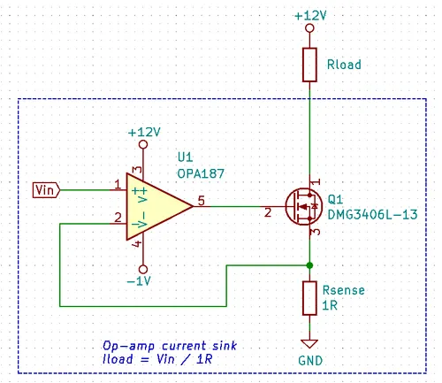
An op-amp can be easily wired up with a MOSFET and sense resistor to make a voltage controlled current source. See Current Sources And Sinks: Op-amp Current Sink for info on how to make an op-amp current source, including schematics, equations and worked examples.
Summing Amplifiers
Op-amps can be used to sum (add) voltages together. There are called summing amplifiers.
Summing amplifiers are used for things such as:
- Mixing audio signals: Audio mixers can be made from summing amplifiers, which combine multiple audio tracks together (e.g. singing with guitar, piano and drums).
- Creating a DAC: Many inputs with resistances following a pattern are used. These days however you should probably just buy a dedicated DAC IC!
- Level-shifting: For example, shifting a +-5V signal to 0-3.3V for input into a DAC. A two input summing amplifier can do this, with one input being the AC signal you want to level-shift and the other input being a fixed DC offset. Combined with the gain of the op-amp you can both offset and scale the signal.
Inverting Summing Amplifier
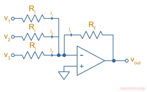
The below schematic shows a inverting summing amplifier with three inputs.
How Does The Inverting Summing Amplifier Work?
The current going through the resistor is just the sum of the currents going through resistors .
The inverting input of the amplifier is at “virtual ground”.
Again, because the inverting input is at , the voltage is just:
Substitute Eq. into Eq. , and then simplify a little:
And there we have it! Eq. shows you [^summing-amplifier-inverting] works as an inverting summing amplifier for three input voltages , , and . Note that aside from summing, the inverting summing amplifier also applies the negative gain , just like a standard [^_inverting_amplifiers, inverting amplifier]. You can make equal to if you don’t want any gain, but you can’t avoid the inverting part. If you don’t want it to invert (perhaps your using a single-sided supply?), then take a look at the [^_non_inverting_summing_amplifier, non-inverting summing amplifier].
Whilst common, the resistors do not need to be equal. If they are not equal, the circuit in [^summing-amplifier-inverting] is called a scaling summing amplifier. Each input voltage is scaled by a value determined by it’s input resistance before being summed together.
Non-inverting Summing Amplifier
The non-inverting summing amplifier is similar to the inverting summing amplifier except that it does not invert the input voltages. The advantages and dis-advantages of the non-inverting vs the inverting summing amplifier are highlighted below:
Advantages
- Does not invert the input signals (this might actually be a dis-advantage, depending on the application!)
- May only need a single-ended voltage supply (depending on the voltage ranges of the inputs).
- Higher input impedance
Disadvantages
- More complicated gain equation/resistor values (because there is no virtual ground at the inputs).
- Unused inputs cannot be left floating, they must be grounded (more on this below).
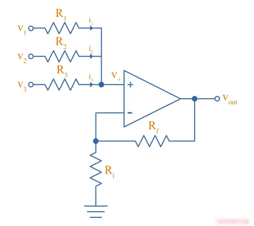
The below schematic shows a non-inverting summing amplifier with three inputs:
If all the input resistors are equal (), the gain equation is:
How Does The Non-Inverting Summing Amplifier Work?
Because we have no nice virtual ground at the non-inverting input, we have to analyze the non-inverting summing amplifier a little differently to the inverting version. First, use Kirchhoff’s current law:
Let’s call the voltage at the non-inverting pin . We can then write replace the currents above with the voltage difference divided by the resistance:
Let’s assume the input resistors are equal (), then simplify and solve for :
So now we have an equation for in terms on the input voltages. As described in the [^_non_inverting_amplifiers], the equation for a non-inverting amplifier is:
Substituting in we get the final equation for a 3-input non-inverting summing amplifier:
Notice the . This scaling factor is equal to the number of inputs the non-inverting summing amplifier has, so remember that the scaling factor changes if you add/remove inputs!
WARNING: Unused inputs into a inverting summing amplifier can be left floating. Unused inputs into a non-inverting amplifier CANNOT be left floating, they need to be tied to ground (0V).
Level Shifters
Op-amps can be used to perform level-shifting. The concept of level-shifting is very similar to what is achieved by [^_summing_amplifiers, summing amplifiers].
Ideal Diodes/Rectifiers
Basic Ideal Diode/Rectifier
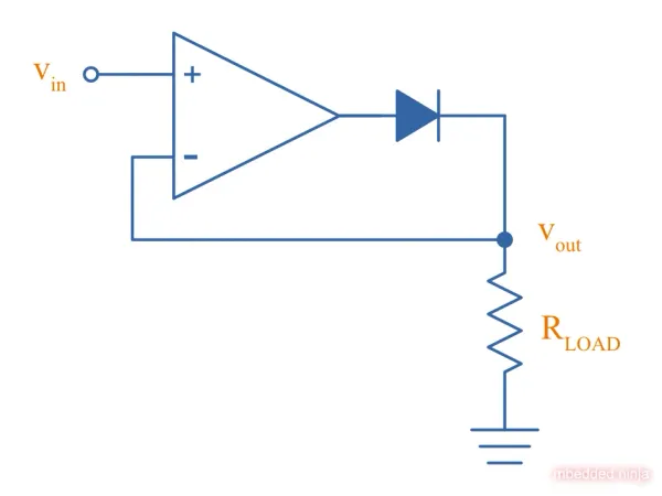
An op-amp can be combined with a regular diode to make an “ideal diode” (also called a superdiode2, precision rectifier, or half/full-wave rectifier), one that rectifies and has no voltage drop. Ideal diode circuits are useful when:
- You have to rectify a signal with precision (the forward voltage drop across the diode is unacceptable).
- You have to rectify a small signal, whose amplitude is less than a forward diode drop.
The below schematic shows the most basic form of an ideal diode (a.k.a. a half-wave rectifier). Because feedback to the inverting pin is taken from the load (), the op-amp will drive it’s output to whatever is needed to make the output voltage the same as the input voltage (when is positive), thereby compensating for the forward voltage drop of the diode. When is negative, the op-amp will try as hard as it can to lower the output voltage, but this will be blocked from the output by the diode, providing the rectifying action.
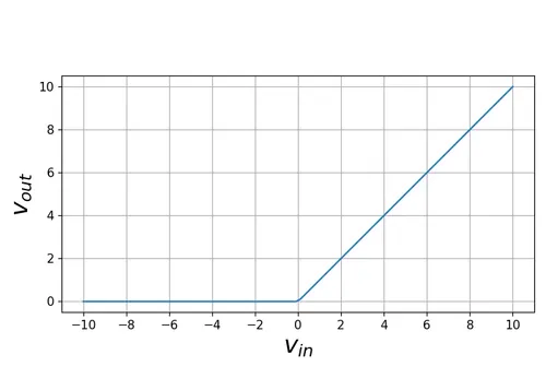
The below graph shows the response of the basic ideal diode circuit.
The ideal diode is only ideal up to a point. It is not limited by the bandwidth and max. slew rates of the op-amp, which is typically much less than of a basic diode! There is also an issue with slew rates with the above circuit. As soon as goes negative, the op-amp will “saturate” and swing it’s output to the maximum negative voltage. This will cause some delay on the output (limited by the slew rate) when the input once again goes positive.
TIP: The standard diode in the ideal diode circuit can be replaced by a Schottky diode for a quick-and-easy speed improvement (Schottky diodes have faster switching speeds).
Improved Half-wave Rectifier
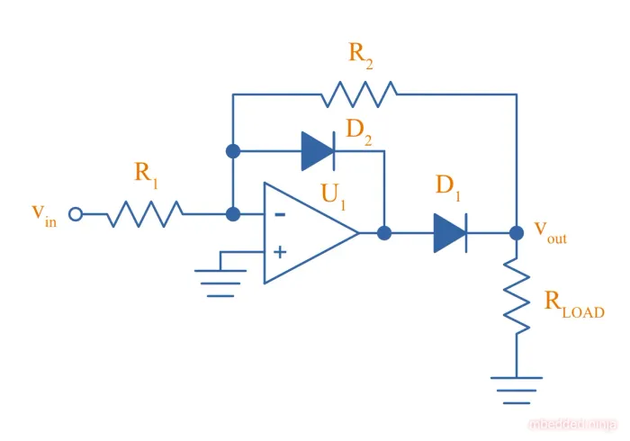
The below schematic shows an improved half-wave rectifier with additional circuitry to prevent the op-amp from saturating when in the blocked part of the cycle3. Note that this also is an inverting half-wave rectifier — it rectifies the negative half of the input and outputs it as a positive wave on the output.
The gain of the half-wave rectifier above is:
Sample And Hold Circuits
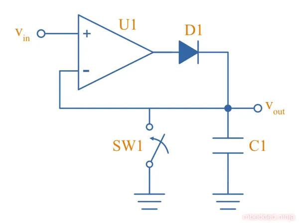
The basic op-amp based sample and hold circuit is an extension of the ideal diode circuit, but with an added capacitor on the output to maintain with the voltage when the input signal is removed.
Important Variables
Sorted by function.
Common-Mode Input Voltage Range
The common-mode input voltage range is the range of voltages that can appear at the input to the op-amp and it still work correctly. For standard single-supply op-amps, the typical range is approximately to . Note how it includes the most negative rail (which is 0V for a single-supply op-amp) but only gets within 1.5V of the most positive rail,
Input Offset Voltage (Vos/Vio)
The input offset voltage (or sometimes called ) is the voltage difference required between the two input pins to force the output to 0. It is a DC measurement parameter. In an ideal op-amp, the op-amp only amplifies a difference between the inputs, and so the output is 0V when the difference is 0V, hence the input offset voltage is 0V. However, real-world op-amps always have some unavoidable differences in the internal components that make up the op-amps (specifically, in the input differential stage of the internal circuitry), and thus the inputs are not perfectly identical. The below circuit shows how the input offset voltage is modelled as a voltage source in series with one of the inputs of an ideal op-amp.
A non-zero input offset voltage results in gain errors between the input and output of a op-amp. The input offset voltage is typically in the following ranges:
- 1-5mV for good general purpose op-amps, 5-15mV for really bad ones.
- 200uV-1mV for specialized low input offset voltage op-amps
- 10uV-200uV for the best “ultra” low input offset voltage op-amps.
- < 1uV for chopper-stabilized (auto-zero) op-amps.
For example, the general purpose LM324 has a typical input offset voltage of 2mV and a maximum of 3mV, at 4. “Low” input offset voltage op-amps will have a in the range of 50-200uV. For example, the OPAx196 family of op-amps has a max. 5.
Input offset voltages vary by op-amp transistor technology. Bipolar op-amps typically have the lowest input offset voltage, followed by CMOS and the BiFET op-amps6.
Input Offset Voltage Drift
The input offset voltage varies with both temperature and time (drift). The variation with temperature is usually represented by (I’ve also seen used7). Typical temperature drift for precision op-amps is in the range of 8. The venerable LM324 has a (max)7.
The change of input offset voltage with time is called aging. Aging is normally specified in . But since aging is a physical process that follows the “random walk pattern” (Brownian motion), it is more accurate to describe it proportional to the square root of elapsed time.
Some op-amps are trimmed by the manufacturer after the op-amp is packaged. Performing trimming after packaging prevents any production-line effects from effecting the input offset voltage. One such example is the family of AD8601, AD8602 and AD8604 op-amps from Analog Devices (they call it DigiTrim). The offset is trimmed with a special digital code using no extra pins (i.e. reuses existing op-amp pins). Once programmed, poly-silicon fuses are blown to permanently set the trim values8.
Trimming Input Offset Voltage
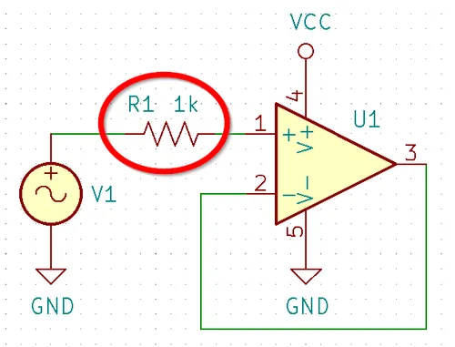
If your op-amp lacks a dedicated trim pin, you can make your own trimming circuit as shown below. This is for an op-amp in the inverting configuration. is a potentiometer, manually adjusted until it cancels out the op-amps input offset voltage.
The maximum input offset voltage you can compensate for with this circuit is given by Eq 8.
Input Bias Current (Ib+ and Ib-)
The input bias current and describe the currents that flow in and out of the op-amps input pins. In an ideal op-amp, no current flows into/out of the input pins (the op-amp has infinite input impedance). In reality, always some small amount of current will flow. Typical input bias currents range from 1-10nA. Special “low input bias current” op-amps can have much lower values. For example, the Texas Instruments OPA396 has a typ. at ! This increases to approx. across it’s entire temperature range (typical)9.
The amount and behaviour of input bias current depends on the op-amp transistor technology. A FET-based op-amp’s input bias current will approximately double with every 10°C rise in temperature10 11.
Input bias currents are a problem because these currents will flow through external circuitry connected to the op-amps inputs. This current when flowing through resistors and other impedances will create unwanted voltages which will increase the systematic errors. Finding an op-amp with a low input bias current can be important for a high sensitivity transimpedance amplifier, such as one connected to a photodiode.
Input Impedance
The input impedance is the internal resistance to ground from the two input pins. In an ideal op-amp, this value is infinite. For most op-amps, this value is somewhere between 1-10MΩ.
Gain-Bandwidth (GBW) Product
The gain-bandwidth product (initialised as GBWP, GBW, GBP or GB) is an important parameter which puts a limit on the maximum gain and frequency an op-amp can operate at. An op-amp’s maximum possible gain reduces as the frequency of the signal increases. The multiplication of the gain with the frequency gives the gain-bandwidth product, which is relatively constant for a particular op-amp.
Hence if the gain bandwidth of a particular op-amp is 1Mhz, and the gain is 10, the maximum frequency that the op-amp can operate linearly at (still provide a gain of 10) is at 100kHz. Or if the gain was set to 100, then the maximum frequency is 10kHz. This also means that an op-amp acts as a low-pass filter, as the gain drops for very high frequencies. Like wise for a GBW of 1MHz, is the gain was just 1 (i.e. acting as a buffer/follower), then it should be able to operate up to frequencies of 1MHz.
An example of an ultra-high gain bandwidth is 1700MHz, which are present in ‘Wideband CFB” op-amps, designed for applications such as RGB line drivers (such as the OPA695). A ‘normal’ GBW can be anywhere between 100kHz and 10MHz. A low gain-bandwidth is around 1kHz (reminiscent of less advanced, older op-amps). Remember gain is unit-less (V/V), so gain bandwidth is expressed as a frequency only. Not realising this can be confusing! The GBW product is closely related to the [^_slew_rate, slew rate].
High Level Output Voltage
The high level output voltage () defines the highest voltage which the op-amp can drive the output to (with respect to the power supply ).
Low Level Output Voltage
The low level output voltage () defines the lowest voltage which the op-amp can drive the output to. The LM324 is rumoured to only be able to drive the output near ground if it is sourcing current, but only to 0.5V minimum if sinking (see this EDA Forum post, LM324 Opamp Gain Instability).
Slew Rate
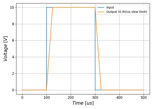
The slew rate of an op-amp defines the maximum rate the output voltage can change with respect to time. In an ideal op-amp, this would be infinite. It has the SI units , and is commonly expressed in . It can be thought of as the slope of the output waveform if one of the inputs of the input was subjected to a step voltage change.
Op-amps have a limited output slew rate due to internal compensation capacitor combined with a finite output drive current. Charing a capacitive output with a constant current (a good approximation) gives a linear increase in voltage (recall that the equation relating voltage to current for a capacitor is ).
The plot below shows how the non-infinite slew rate of an op-amp distorts the shape of an input square-wave “pulse”. The slew rate of (which is not particularly good by any standard) of the “jellybean” LM324 op-amp was used in this plot12.
The max. slew rate of an op-amp limits the amplitude of output waveforms it can produce at high frequencies without distortion. This parameter usually increases as the GBW of the op-amp increases. Higher slew rate op-amps also tend to have higher quiescent currents.
Slew Rate Equation
The maximum frequency of a signal that an op-amp can output before it gets distorted because of it’s maximum slew rate limit is given by the following equation:
where:
is the slew rate, in
is the maximum frequency (of a sine wave) that is allowed before distortion, in
is the peak voltage of the sine wave (i.e. amplitude, or half the peak-to-peak voltage), in
Proof
A sine wave at frequency and has peak voltage is described with the equation:
The slope at any point in time is found by taking the derivative. As per standard derivative rules, the derivative of is and you multiply the function by what is inside the :
We want to find the maximum slope, . We know that the maximum value of any function is , so we can simplify to:
This maximum slope is the maximum slew rate of the op-amp . Hence:
Slew Rate Effects On Sine Waves
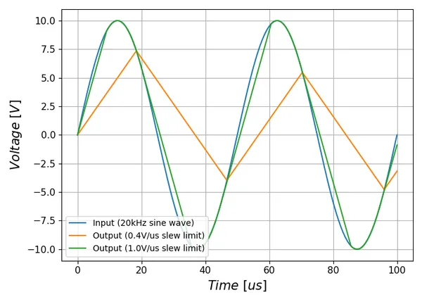
The below plot shows different levels of distortion for a 10V (peak) 20kHz sine wave when it is generated by an op-amps with different slew rates. The jellybean LM324 slew rate of is shown (which outputs a triangle wave!) along with a slightly better (which just clips the sine wave). The minimum slew rate required to prevent any distortion of the sine wave is .
Quiescent Current
The quiescent current (current with no load, device in steady-state) is generally constant over the total rated supply voltage range. Obviously, if there is a load on the op-amp, the current drawn through the power pins (the supply current) will be the sum of the quiescent current and the current going through the load.
Quiescent currents for standard op-amps are typically between 1.5-4mA. A ‘low-power’ op-amp has a typical quiescent current between 0.5-1.5mA (such as the LM258N). Then there are ultra-low power op-amps that only draw 5-20pA (such as the LMC6464). You normally sacrifice slew-rate and gain-bandwidth for ultra-low power. Likewise, higher gain-bandwidth and higher slew rate op-amps typically have larger quiescent currents.
Cascading Op-Amps
Cascading op-amps is concept when the output of one op-amp is connected to the input of another. There can be an arbitrary number of op-amps in the cascade, but usual limits are 3-4.
For a fixed-gain, cascading op-amps can also be used to increase the bandwidth, as each individual op-amp now can operate at a lower gain and therefore has a larger bandwidth as defined by the gain-bandwidth product. Note though that each additional op-amp added to increase the bandwidth gives diminishing returns. Also important to note that op-amp bandwidth is defined as the -3dB gain points. Hence the bandwidth does not stay the same (total bandwidth gets smaller) when two identical op-amps are cascaded, as these will now the -6dB points. A practical limit for fixed-total-gain increased-bandwidth cascading is about 3-4 op-amps.
The Gain
When cascading op-amps, the total gain is the product of all of the individual op-amps gains, i.e.:
The Bandwidth
The bandwidth of cascaded op-amps is not as simple to calculate as the gain.
If all of the op-amps are identical, then the following equation can be used:
where:
= the total bandwidth of the cascaded op-amp system
= the bandwidth of the individual op-amps (remember, they have to be identical)
= the number of op-amps in the cascaded system
The above equation gives diminishing returns with every additional op-amp added.
Feedback Resistor Values
As a rule-of-thumb, you should use the lowest acceptable resistances in op-amp feedback paths to reduce instabilities.
Types Of Op-Amps
General Purpose
General purpose op-amps typically have parameters in the following ranges:
- Gain Bandwidth Product: 1MHz
- Input Bias Current: 15pA
- Input Voltage Offset: 1mV
- Output Current: 20-50mA
- Icc: 1mA
Rail-to-Rail Op-Amps
A rail-to-rail op-amp is an op-amp which supports input voltages near the power rails, and can drive the output close to the one or more of the power rails. We must stress the word NEAR, as the op-amp’s output voltage will never get exactly to the rail, due to the finite voltage drop across the output-stage transistors. Rail-to-rail op-amps just support wider ranged input voltages and can drive closer to the rails than general purpose op-amps can. Look for the low level output voltage () parameter in the op-amp’s datasheet. For “rail-to-rail” op-amps, this will usually be about 100-200mV about ground at normal load currents.
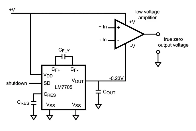
This also means that a rail-to-ral single-supply op-amp cannot output 0V. To achieve a true ground output, you need a negative voltage supply. There are dedicated ICs designed to provide a small negative power supply to op-amps so that they can output true ground. One such example is the Texas Instruments LM7705, a “Low Noise Negative Bias Generator”. This IC only generates -230mV, which allows the designer to use CMOS-based op-amps which usually have a maximum supply voltage of 5.5V.
Micropower Op-Amps
Micropower is a termed used for extremely low quiescent current op-amps that are designed for battery or energy recovery-based power supplies. The supply current of micropower op-amps is typically within the range of 50-100uA at a supply voltage of 2-10V. Because they are designed for battery-based systems, they are also commonly single-supply op-amps.
Instrumentation Amplifiers
Instrumentation amplifiers are analog voltage amplifier circuits that, although are drawn the the same symbol as an op-amp, are typically made up internally from three op-amps (and passives). You can either make an instrumentation amplifier out of discrete op-amps or purchase a instrumentation amplifier IC which contains all the op-amps within the same chip.
Manufacturer Part Number Families
-
INA ** INAx126: Precision instrumentation amplifiers by Texas Instruments. The INA126 has one amplifier per package, the INA2126 has two. ** INA290: Precision current-sense amplifier.
-
LM741: Very popular and old “741” style op-amp produced by Texas Instruments, ON Semiconductor and Rochester Electronics.
-
LT: The prefix Linear Technology (now Analog Devices) uses for their range of op-amps. ** LT1006: Precision, single-supply op-amp. ** LT1077: Micropower, single-supply op-amp. ** LT1167: Instrumentation amplifier.
-
MAX: Op-amps by Maxim. ** MAX4194: Instrumentation amplifier.
-
OP07: Analog Devices/Texas Instruments ranges of low input offset voltage op-amps. ** OP07C: ±3-18V VCC, -40 to +85°C industrial temp. range *** OP07CP: DIP-8 package *** OP07CS: SOIC-8 package ** OP07D: ±4-18V VCC ** OP07E: 0 to 70°C commercial temp. range
-
OPA: Texas Instruments (previously Burr-Brown) family of op-amps. ** OPAx187: Zero-drift 36V rail-to-rail op-amps. Includes the OPA187 (1 op-amp), OPA2187 (2 op-amps) and OPA4187 (4 op-amps). ** OPA241: Single-supply ** OPA251: Dual-supply ** OPA27: Texas Instruments (previously Burr-Brown) family of ultra-low noise, precision op-amps. Internally compensated for unity-gain stability. ** OPA37: Uncompensated version of the OPA27.
-
TLE202: Texas Instruments family of “high-speed low-power” precision operational amplifiers. Belong to the Excalibur family of TI op-amps which uses “isolated vertical PNP transistors” to give unity-gain bandwidth and slew rate improvements.
-
TLV: Texas Instruments family of op-amps.
-
Vsupply is voltage from Vdd/Vcc to Vss/Vee.
The Different Types Of Gain, Explained
Open-loop gain (sometimes written as ) is the gain of the op-amp without any feedback.
Closed loop gain is the over-all gain of the op-amp with feedback.
We can generalize the circuit of an op-amp with negative feedback to the block diagram shown below.
From the above block diagram we can write an equation for :
What we are really interested is an equation for the closed-loop gain which is equal to …all we need to do is to re-arrange the equation as shown below:
And so we come to an equation for the closed loop gain as:
We can take this one step further, since normally the open-loop gain for an op-amp is very large, in the range of to . With that, we can simply the closed loop gain to be:
In summary:
- Open-loop gain:
- Loop gain:
- Closed-loop gain:
Examples
Below are some examples of op-amps that stand out from the crowd for some reason, be it popularity, years in service, or functionality wise.
AD860x
US$3.50 (1) Good for high precision stuff! Awesome for photo-diode amplification (both current-to-voltage and voltage-to-voltage configurations).
LM32x
A common family of op-amps that has been around for along time, they can operate of a single supply and can swing right to ground, but cannot swing to the rail voltage. The LM321 has one op-amp, the LM328 has two (dual), and the LM324 has 4 (quad).
LM833
One of the cheapest ‘audio’ op-amps available (about US$0.20 as of 2011). Features a high GBW for it’s price.
OPA695
US$3.50 (1) This is a ultra-wideband, current-feedback op-amp. If you need an op-amp with a ridiculously high gain-bandwidth product, this is along the lines of what you want to use. It has a GBW of 1700Mhz and a maximum slew-rate of 4300V/us.
OP07
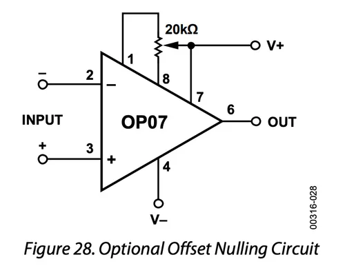
A op-amp with a “ultra” low input offset voltage (resistors are trimmed at production time to achieve this), guaranteed to be no more than 75uV. This op-amp also features offset nulling pins to further reduce the input offset voltage by performing trimming once the op-amp is installed in a circuit.
Negative Voltage Rails
Dedicated charge-pump topology power supply ICs are available that supply a small negative voltage to the op-amps V- pin.
Isolation Amplifiers
Isolation amplifiers provide galvanic isolation between the input (sensor) and output (measurement circuitry). They are used to protect the sensor measurement and recording circuitry (e.g. a microcontroller with on-board ADC) from dangerously high voltages at the sensor, and also the opposite, to protect the sensor environment from potentially dangerous voltages on the rest of the system.
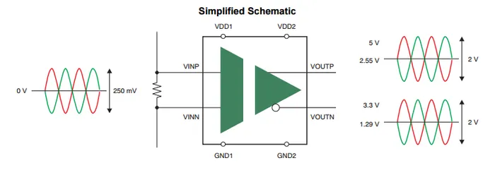
A common application would be to isolate and amplify the voltage across a current-sense resistor on a high-power motor, or to protect humans with medical sensors connected to them from the measurement system.
Basic isolation amplifiers require two power supplies (one for each side of isolation), while others incorporate built-in transformers so that you only have to provide one power source.
Input Resistors
One of the first things you learn about an op-amp is that the input impedance on the input pins are very large (ideally infinite). So naturally you would start to question why resistors would be connected to the input pins of an op-amp like shown below.
These input resistors serve to limit the input current if the voltage on the input pin goes above . Most op-amps have protection/clamping diodes from the input pins to (typically you can determines this if in the datasheet the input pins max voltage is rated to , which is one diode voltage drop). If there was no resistor there, the built-in diode would conduct and sink a large current from the input pin to , possibly damaging the op-amp. The resistor limits this current to a safe value.
Offset Nulling Circuits
Some op-amps which are designed to have very low input offset voltages also come with offset nulling pins to further trim the input offset voltage once the op-amp is installed in circuit. The OP07 is one op-amp which has these pins. Typically, a potentiometer is connected across these pins with the wiper going to , as shown below.
Negative Impedance Converters (NICs)
What Is A NIC?
A negative impedance converter (NIC) is a clever op-amp circuit which creates negative impedance (you might be wondering what negative impedance actually is, more on this later). A NIC can be constructed from an op-amp and a few passive components as shown in the following schematic:
Typically the two resistances are the same (), and then the input impedance is:
where:
is the input impedance, in Ohms ()
is the impedance of the component connected between the inverting terminal and ground, as shown on the diagram, in Ohms ()
What Does Negative Impedance Actually Mean?
What does negative impedance actually mean? If is just a simple resistor with resistance (the most basic kind of NIC), then the impedance is . This means the circuit behaves just like a simple resistor connected to ground, except that the current comes out of the resistor, not into it.
Things get more interesting when you replace this resistor with a capacitor.
TODO: Add explanation of what happens when capacitor is added.
NIC Input Impedance Proof
To prove , we need to find the input current at inverting terminal, and then use . The input current can be found by application of Ohm’s law and the golden rules of op-amps. Using the rule that the voltage at the two input terminals will be the same, we know the voltage across the impedance is going to be:
Using Ohm’s law, the current through the impedance is therefore:
Because there is no current going into the inverting terminal of the op-amp, this current must also be flowing through :
Now knowing the voltage at the inverting terminal and the current through we can write an equation for the voltage at the output of the op-amp:
Now that we know the voltage on both sides of we can find the voltage across it:
Now we know the voltage across we can find the current going through it using Ohm’s law:
Because the voltage on the right-hand side of is higher, this current is flowing right-to-left. Since no current flows into the inverting terminal of the op-amp, this also must be current flowing “out” of the input terminal. Thus:
Knowing the input current and voltage, we can finally write an equation for :
Proof complete!
Chopper-Stabilised Op-Amps
TODO: Add info.
Capacitive Loading
TODO: Add info.
Industry Standard Package Pinouts For Op-Amps
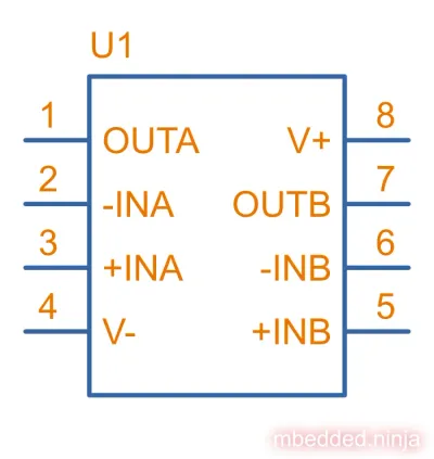
Op-amps are usually packaged in industry standard through-hole and surface mount packages. For many of these packages, there are industry standard pinouts which means you can easily find pin-compatible alternatives for any given op-amp. This section aims to illustrate some of these industry standard pinouts.
For 8-pin packages:
Footnotes
-
Electronics Tutorials. Operational Amplifiers - The Differential Amplifier. Retrieved 2023-08-29, from https://www.electronics-tutorials.ws/opamp/opamp_5.html. ↩
-
Keim, Robert (2018, Feb 8). When a Diode Simply Isn’t Good Enough: The Superdiode. AllAboutCircuits. Retrieved 2021-09-27, from https://www.allaboutcircuits.com/technical-articles/when-a-diode-simply-isnt-good-enough-the-superdiode/. ↩
-
Ducu, Dragos. (2011). AN1353: Op Amp Rectifiers, Peak Detectors and Clamps. Microchip. Retrieved 2021-10-01, from http://ww1.microchip.com/downloads/en/AppNotes/01353A.pdf. ↩
-
Texas Instruments (2015). LMx24-N, LM2902-N Low-Power, Quad-Operational Amplifiers. Retrieved 2020-10-20, from https://www.ti.com/lit/ds/snosc16d/snosc16d.pdf. ↩
-
Texas Instruments (2017, Jul). OPAx196 36-V, Low-Power, Low Offset Voltage, Rail-to-Rail Operational Amplifier. Retrieved 2021-09-03, from https://www.ti.com/lit/ds/symlink/opa196.pdf. ↩
-
Palmer, Richard (2001). DC Parameters: Input Offset Voltage (Vio). Texas Instruments. Retrieved 2020-10-20, from https://www.ti.com/lit/an/sloa059/sloa059.pdf. ↩
-
OnSemiconductor (2021, Aug). Single Supply Quad Operational Amplifiers (Datasheet). Retrieved 2021-09-03, from https://www.onsemi.com/pdf/datasheet/lm324-d.pdf. ↩ ↩2
-
Analog Devices (2008, Oct). MT-037: Op Amp Input Offset Voltage. Retrieved 2021-09-03, from https://www.analog.com/media/en/training-seminars/tutorials/MT-037.pdf. ↩ ↩2 ↩3
-
Texas Instruments (formally Burr-Brown) (2021, Jul). OPA396 Precision, Low IQ, Low Input Bias Current Op Amp (datasheet). Retrieved 2022-10-10, from https://www.ti.com/lit/ds/symlink/opa396.pdf. ↩
-
Analog Devices (2008, Oct). Op Amp Input Bias Current. Retrieved 2020-10-20, from https://www.analog.com/media/en/training-seminars/tutorials/MT-038.pdf. ↩
-
Luis Orozco (2014). MS-2624: Optimizing Precision Photodiode Sensor Circuit Design. Analog Devices. Retrieved 2022-02-24, from https://www.analog.com/en/technical-articles/optimizing-precision-photodiode-sensor-circuit-design.html. ↩
-
Texas Instruments (2014). LM321 Low Power Single Operational Amplifier. Retrieved 2021-10-02, from https://www.ti.com/lit/ds/symlink/lm321.pdf. ↩ ↩2


