Xilinx 7 Series Design Guide
This is in no way meant to replace the comprehensive Xilinx design guides for 7 Series devices, but rather serve as a quick reference guide along with tips and tricks which may not be obvious from reading the official Xilinx material.
IO
The pins in a bank are labelled something like IO_L14P_T2_SRCC_14. What does this mean?
| IO | This pin can be used as general IO. |
| L14P | This pin is part of a differential pair. The pair number is 14, and this is the positive (P) pin. |
| T2 | The pin is part of bank T2. |
Decoupling Capacitors
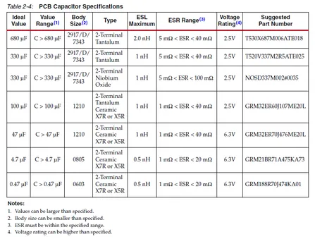
Xilinx gives strict recommendations on the parameters of the capacitors used for decoupling. The following image shows a table with the ESL, ESR and body size limits for the various-valued capacitances.
The Kintex and Virtex-7 devices has some in-built decoupling capacitors for the larger package sizes (you still need to add external decoupling caps, just not as many).
Reverse-aspect capacitors can be used for when ultra-low parasitic inductances are required.
Un-used I/O Banks
Using a large device for a small project could mean that there are entire banks of unused I/O pins. In these cases you are allowed to leave the bank’s Vcco pins (e.g. Vcco_14) and I/O pins disconnected. However, for ESD reasons, it is better to connect these pins to either (in order of preference): GND, a valid Vcco voltage, or a floating plane.
MGTs
The Xilinx 7 Series FPGAs have in-built Multi-Gigabit Transceivers (MGTs). These are SerDes capable of 1Gbps+ transmission rates.
The MGTs on-board a 7 Series FPGA can be used to implement high-speed communication protocols such as PCIe (PCI Express).
The MGTs have decision-feedback equalisation (DFE) blocks, which aim to reduce the reduce the inter-symbol interference (ISI) on the current symbol.


