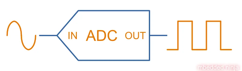
Analogue-to-Digital Converters (ADCs)

An analogue-to-digital converter (ADC) is a device which converts an input analogue voltage level into a representative digital value. They are commonly used in embedded electronics to measure things such as values from an analogue sensor or voltage rails (typically fed through resistor dividers). They are very popular and many microcontrollers have one or more built-in ADCs, with each ADC having multiple inputs (5 to 12 is common) shared with GPIO. You can also get stand-alone ADC ICs which normally offer greater precision and resolutions.
Microcontroller ADCs
Microcontroller ADCs usually have an 8–12 bit resolution (with some going up to 20-bit). A typical microcontroller has only one ADC unit, but offers an input multiplexor to be able to select an analogue input from a number of pins. The ADC is controlled via registers, usually with voltage reference selectable from an external pin or an internal reference. Voltage dividers can be used to scale a larger voltage into the range acceptable to the microcontroller. Since the input to the ADC is usually of a very high impedance, the voltage at the ADC pin will be related to the ratio of the resistances in the resistor divider. A pull-down resistor is usually connected to an ADC input to prevent it from floating (and giving erroneous results when nothing is connected).
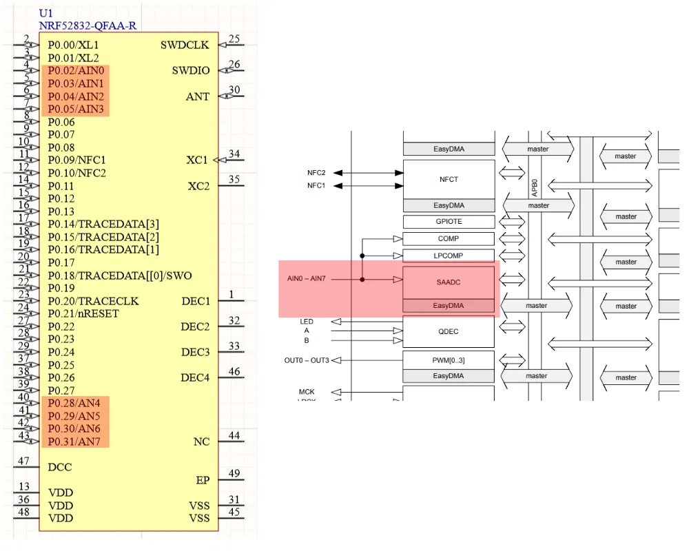
On the left-hand side of the below image is a schematic diagram of a Nordic nRF52 MCU with the ADC pins highlighted. There are 8 ADC channels, AIN0 through AIN7 (4 to 7 are called ANx not AINx for some reason). Firmware can connect any one of these channels to the internal ADC peripheral which can then measure the voltage at that pin. The right-hand side shows the same ADC peripheral in the MCU’s block diagram.
Accuracy And Resolution
The resolution of an ADC normally depends on the number of bits it supports. ADCs typically support a bit resolution of 8 to 24 bits, with the resolution error usually limited to the last bit. The accuracy can normally be increased by increasing the sample time, which lengthens the amount of time the input capacitor has to stabilize and allows the ADC to complete finer adjustments. Accuracy can also be increased by taking multiple samples and averaging them. A good way to do this with a microcontroller is to take a number of samples equal to a power of two, (i.e. 2, 4, 8, 16, …), and then to save computational time the result can be bit shifted right times instead of using the divide function (essentially doing the same thing).
Measuring Techniques
There are many ways to convert an analogue signal into a digital one. The two most popular ADC methodologies are successive approximation register (SAR) and Delta-Sigma. SAR ADCs are usually faster but have a lower resolution (typically 8 to 12-bit) while Delta-Sigma ADCs are slower but offer greater accuracy (typically up to 20-bit). SAR ADCs typically have a sampling rate of 100kHz-1MHz while Delta-Sigma ADCs have a sampling rate of 1-20Hz.
Delta-Sigma ADCs also take longer to switch between input signals (if measuring multiple signals with just one ADC) because they incorporate a filter which needs to be reset and stabilised before the measurements become accurate (essentially the filter’s response time).
Switched Capacitor Array
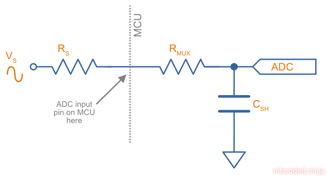
Many SAR ADCs use the switched capacitor array architecture1. Internally, they have a multiplexor to select from one of many input signals (separate pins on a dedicated ADC IC, or shared with GPIO on a MCU). One input is selected and is connected to the sample-and-hold capacitor . The length of time it is connected to this capacitor is called the acquisition time or sample time.
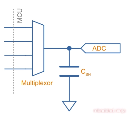
The internal capacitance is also called 2. The capacitance is small and normally in the range of 2 pF to 10 pF. For example, the for the STM32G491KE MCU is 5 pF2.
On many MCU SAR ADCs the sample-and-hold capacitor is not discharged between successive measurements — for example, this is the documented behaviour of the STM32G4 family3. Other architectures do precharge or reset before each acquisition, so check your datasheet rather than assuming.
Where the capacitor is not reset, each acquisition starts at the voltage the previous sample finished at. The S/H capacitor then has to be driven from that residual voltage to the new input within the acquisition time, through the on-resistance of the input multiplexor and the source impedance. If the acquisition time is too short relative to that RC, the new sample doesn’t fully settle and the result is biased by the previous one — a form of channel-to-channel cross-talk.
There are several common mitigations:
- Increase the acquisition (sample) time so that the input network has plenty of RC time constants to settle. Cheapest fix when the ADC’s sample-rate budget allows it.
- Sample each channel twice and discard the first reading — the first sample drags most of the way to the new input voltage, so the second sample only has to close a much smaller gap. The residual error is reduced, but not eliminated. Halves throughput, but works without any hardware changes.
- Interleave a known internal channel into the scan sequence — most MCU ADCs expose an internal ground rail or via the same input multiplexor. Converting that internal channel between each pair of real channels drags to a known, channel-independent voltage (typically through a very low internal source impedance, so it settles fast). The next real measurement still has to charge from that starting point, but the residual error is now predictable and the same for every channel rather than “whatever the previous channel happened to be”. This halves the throughput like the “sampling each channel twice” method. Some ADCs go one better and offer a built-in reset/precharge step in their conversion sequence — when available, that’s the cleanest option of all.
- Add an external capacitor on the input pin (much larger than ) to act as a local charge reservoir, so the S/H step barely moves the input voltage. Best when source impedance is high and you can’t afford to lengthen the acquisition time.
The TI application report Switched-Capacitor ADC Analog Input Calculations1 is a great walk through of how to calculate the maximum permissible source resistance given a desired accuracy in LSB for an ADC.
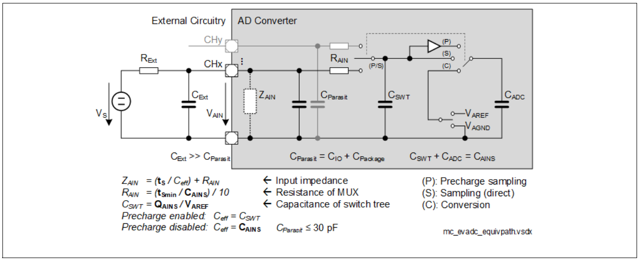
Models of ADC input circuitry can get complex! The below image shows the input model for the Infineon AURIX TriCore TC33xEXT AA family of MCUs.
Medical Uses
ADCs are commonly used in medical devices for biopotential measurements. One common application is for the analogue front-end in EEG devices. The Texas Instruments ADS1299 is one example of an ADC IC designed for EEG applications.5
4-20mA Current Loops
ADCs can be used to read the value from a 4-20mA current loop signal with the help of a current-to-voltage converting resistor (what all resistors do, right?).
See the 4-20mA Current Loops page for more info.
Isolated Voltage Measurement
You can use isolated amplifiers to measure voltages which you want to remain isolated from the ADC/MCU. A common use case would be to measure mains voltages (110-400 VAC) with an ADC. You can buy standalone ICs which contain both an isolated analogue amplifier and an isolated power supply. The isolated power supply is used to power the isolated side of the amplifier without requiring an additional isolated PSU (without this, you would need a power supply for each side of the isolation barrier).
One example of an isolated amplifier IC is the Texas Instruments AMC3330. A typical application circuit for it is shown in This is a placeholder for the reference: fig-amc3330-isolated-amplifier-ic-typical-application-circuit. The isolated side shows a resistor divider from an AC source such as mains voltage used to scale down the voltage to an amplitude of 1.0 V.6
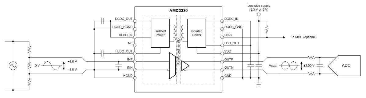
By nature of the measurement being isolated, it is not ground referenced and thus on the MCU side there is a differential signal. You could either connect one side to GND if you want to use a single ADC pin (and you were sure the signal only went in one direction), or use a differential ADC input.
Examples
Texas Instruments ADS8866IDRCR
| Parameter | Value |
|---|---|
| Manf. | Texas Instruments |
| Manf. Part Num | ADS8866IDRCR |
| Topology | SAR |
| Resolution | 16-bit |
| Speed | 100ksps |
| Digital Interface | SPI |
| Package | DFN-10-3x3-TP |
Claims to be pin compatible with the Microchip MCP33131-05-E/MN, however the analogue supply voltage ranges are incompatible!
Microchip MCP33131-05-E/MN
| Parameter | Value |
|---|---|
| Manf. | Microchip |
| Manf. Part Num | MCP33131-05-E/MN |
| Topology | SAR |
| Resolution | 16-bit |
| Speed | 500ksps |
| Digital Interface | SPI |
| Package | DFN-10-3x3-TP |
Suppliers
Footnotes
-
Tom Kugelstadt (1998, Sep). Switched-Capacitor ADC Analog Input Calculations Application Report. Texas Instruments. Retrieved 2024-02-11, from https://www.ti.com/lit/an/slaa036/slaa036.pdf. ↩ ↩2
-
STMicroelectronics (2021, Sep). STM32G491xC/STM32G491xE - Arm® Cortex®-M4 32-bit MCU+FPU, 170 MHz / 213 DMIPS, up to 512 KB Flash, 112 KB SRAM, rich analog, math accelerator [datasheet]. Retrieved 2024-02-12, from https://www.st.com/resource/en/datasheet/stm32g491ke.pdf. ↩ ↩2
-
STMicroelectronics. STM32G4: ADC sampling and hold capacitor value [forum post]. Retrieved 2024-02-12, from https://community.st.com/t5/stm32-mcus-products/stm32g4-adc-sampling-and-hold-capacitor-value/td-p/145004. ↩
-
Infineon (2021, Mar). AURIX TriCore TC33xEXT AA MCU Family Datasheet [datasheet]. Retrieved 2024-03-26, from https://www.infineon.com/dgdl/Infineon-TC33xEXT_AA-step_DataSheet-DataSheet-v01_01-EN.pdf?fileId=8ac78c8c82ce566401833cdf75272dba. ↩
-
Texas Instruments. ADS1299: Low-Noise, 8-Channel, 24-Bit Analog-to-Digital Converter for Biopotential Measurements [product page]. Retrieved 2026-05-29, from https://www.ti.com/product/ads1299. ↩
-
Texas Instruments (2024, Aug). AMC3330 Precision, ±1V Input, Reinforced Isolated Amplifier With Integrated DC/DC Converter [datasheet]. Retrieved 2025-06-10, from https://www.ti.com/lit/ds/symlink/amc3330.pdf. ↩ ↩2