PCIe Hardware Design Guide
This page contains information useful to hardware designers using a PCIe bus as part of their PCB design.
The PCIe physical layer can be split into two sub-layers, the electrical and logical layers.
Electrical Sub-Layer
The pinout for a x1 PCIe connector are as follows:
| Pin Number | Side B Pin Name | Side B Description | Side A Pin Name | Side A Description |
|---|---|---|---|---|
| 1 | +12V | +12V power (from host) | PRSNT#1 | Hot plug presence detect |
| 2 | +12V | +12V power (from host) | +12V | +12V power (from host) |
| 3 | +12V | +12V power (from host). Note: This used to be RSVD, but was changed to +12V in PCIe revision 1.1). | +12V | +12V power (from host) |
| 4 | GND | Ground | GND | Ground |
| 5 | SMCLK | SMBus clock | JTAG2-TCK | JTAG clock |
| 6 | SMDAT | SMBus data | JTAG3-TDI | JTAG data in |
| 7 | GND | Ground | JTAG4-TDO | JTAG data out |
| 8 | +3.3V | +3.3V power | JTAG5-TMS | |
| 9 | JTAG1-TRST# | JTAG reset | +3.3V | +3.3V power |
| 10 | +3.3V-AUX | Auxilary +3.3V power. | +3.3V | +3.3V power |
| 11 | WAKE# | Link re-activation | PWRGD (PERST#) | Power good. May also be called PERST# (which stands for NOT power reset). |
| MECHANICAL KEY | ||||
| 12 | RSVD | Reserved | GND | Ground |
| 13 | GND | Ground | REFCLK+ | Reference clock positive (output w.r.t host) |
| 14 | PETp0 | Transmitter lane 0, positive | REFCLK- | Reference clock negative (output w.r.t host) |
| 15 | PETn0 | Transmitter lane 0, negative | GND | Ground |
| 16 | GND | Ground | PERp0 | Receiver lane 0, positive |
| 17 | PRSNT#2 | Hotplug detect 2 | PERn0 | Receiver lane 0, negative |
| 18 | GND | Ground | GND | Ground |
Pin B3 used to be RSVD, but was changed to +12V in PCIe revision 1.1 (March 2005). For all new designs it is recommended to connect it to +12V.
The card-edge finger for A1 (PRSNT1#, hot-plug detect 1) and B17 (PRSNT#2, hot-plug detect 2) is shorter than all of the others, hence they should be the last two pins to make contact.
Differential-Pair Routing
Individual traces for a given differential pair must be matched in length to a tolerance of 0.127mm (5mils).
The spacing between traces of different pairs must be at least 0.508mm (20mils) (edge-to-edge) to reduce cross-talk effects.
Trace length matching between pairs is not required because the PCIe specifications allow for up to 8ns of skew between differential pairs (e.g. between REFCLK and PET0).
Vias in the differential pairs should be avoided as much as possible. If they cannot be avoided, then the via pad size should be less than 0.635mm (25mils) and the hole size less than 0.356mm (14mils).
Regular FR4 PCB material can be used with PCIe traces.
Differential-Pair Decoupling Caps
The PCIe standard states that AC coupling capacitors must connected in series on the transmitting side of all differential data pairs. The capacitance must be between 75 and 200nF. 100nF 0402-sized capacitors are recommended. The capacitors must be placed as close to the transmitting side as possible to reduce discontinuity effects.
Thus, for daughter-board with a slave PCIe port, decoupling caps need to be placed on the PER differential signals.
Terminating Resistors
Most PCIe-compatible IC’s automatically embed the 50Ω terminating resistors inside themselves, meaning no external termination is required.
Bootup Timing
The PERST# net is deasserted by the master 100ms after a daughter board is first powered up (again, power comes from the master, in the form of +3.3 and +12V). The daughter board must be ready to link train (i.e. communicate other the PCIe port), no more than 20ms after PERST# is deasserted. Thus the daughter board has to be ready for PCIe communications 120ms after it is first powered up.
With PCIe ports implemented on large FPGA-based designs, this can be a challenging design constraint. An FPGA which loads its bitstream (configuration data) from external flash over a SPI bus using standard data rates can easily take more than 120ms. Fortunately there a few ways to speed up the FPGA configuration: 1. Use x2 or x4 SPI memory. 2. Use a faster SPI clock speed (e.g 100MHz rather than 50MHz). Note that at these times sometimes the routing needs to be treated as a transmission line. 3. Use compression to reduce the size of the bitstream. 4. The loading/configuring of a PCIe-related bitstream, which quickly makes the PCIe port functional, followed by the loading/configuring of the rest of the FPGA system. Xilinx calls this Tandem PCI Express or_ Tandem PROM_.
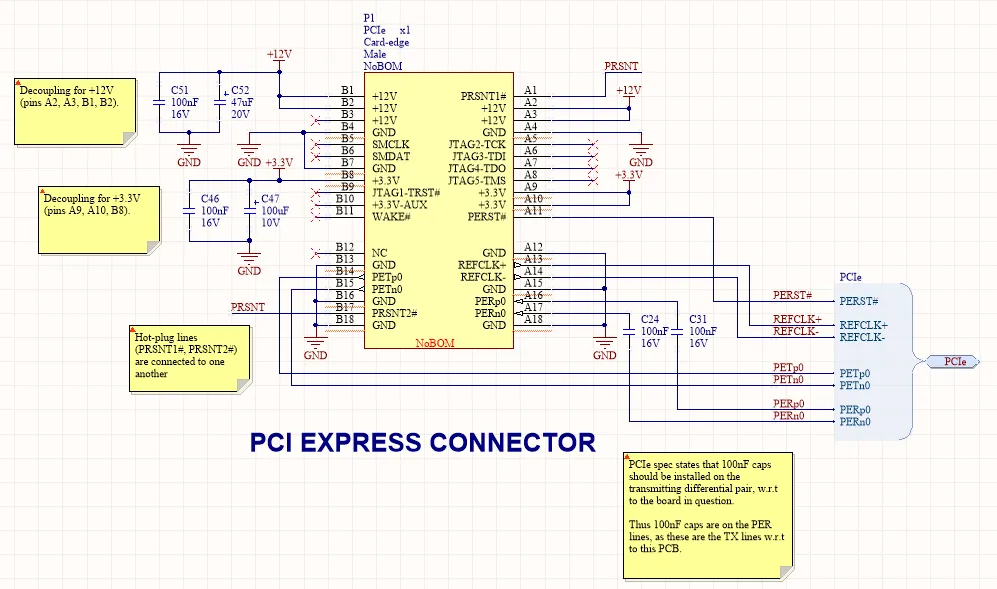
Example PCIe x1 Card-Edge Schematic Design
The following image shows an example PCIe x1 card-edge connector schematic symbol and associated components:


