EMC Design Guidelines

SMPS EMC Guidelines
Switch-mode power supplies (SMPS) can be a large source of EMI in a circuit, which can cause your PCB to fail EMC tests. Most of the noise is emitted at the switching frequency and it’s harmonics. Many manufacturers will provide recommended layouts for their SMPS ICs and surrounding components, and it’s generally a good idea to follow these as closely as possible in your design. This includes things such as:
- Input and output capacitors as close as possible to the SMPS IC.
- Keeping the current loops involving the capacitors, inductor(s) and switching node(s) as small as possible (w.r.t. to their area).
- Making sure there is a continuous ground plane close to all other nets (this also relates to keeping current loops small).
Hot Loops
Hot loops are the current loops in SMPS designs which generally generate/radiate the most EMI and are of greatest concern when it comes to EMC.
The following image shows a basic buck converter circuit (with the switch representing a MOSFET and using a flyback diode rather than active rectification). The light blue rectangle shows the current path when the switch is closed. The green rectangle shows the current path when the switch is open. The red rectangle shows the “hot loop”, the current path which has the highest di/dt and is generally the loop you want to minimize and pay particular care to when routing the tracks.
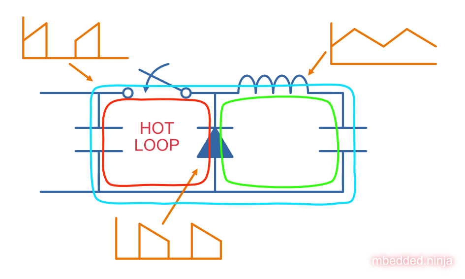
The loop involving the inductor and output capacitor are not so important because they experience a relatively smooth trapezoidal shaped current profile (at least when in continuous conduction). The input capacitor and switch however experience a much larger di/dt — when the switch is closed it goes from 0A and jumps up to the current through the inductor. It then follows the inductor current on the upwards rise until the switch is opened, at which point the current rapidly falls back to 0A. The diode is in a similar position, except it conducts when the input cap and switch are not (it takes the falling edge of the inductor current). Thus the “hot loop” creating the most EMI is the loop involving the input capacitor, switch and diode1.
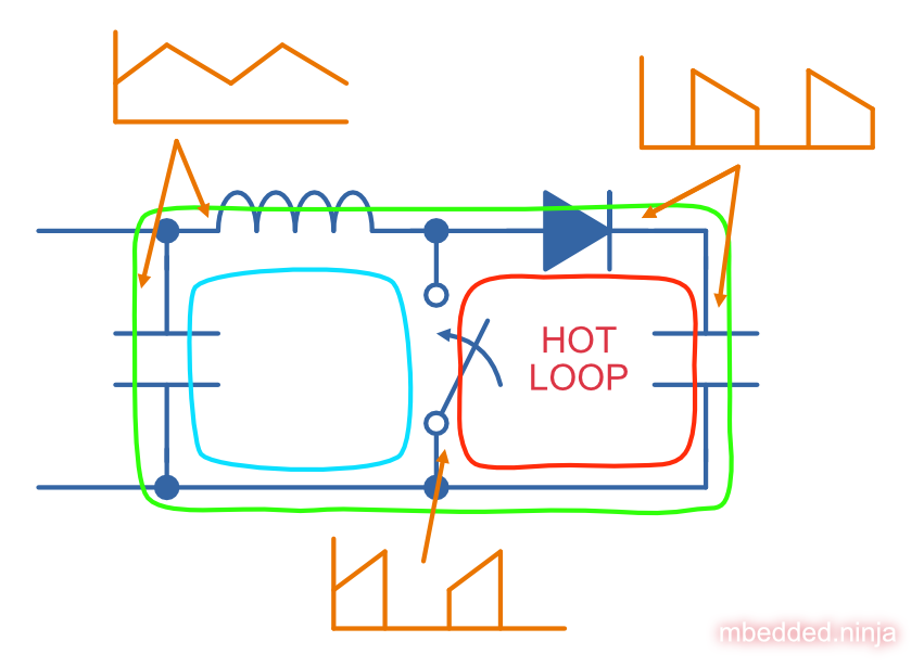
The hot loop for a boost converter is on the output side rather than the input:
Inductor Polarity
Inductors don’t have a polarity right? Most of the time, they don’t. But certain inductors do feature polarity marks for EMC purposes.
When inductors are used in switch-mode power supplies, one side of the inductor is normally connected to what is called the switching node. In a buck converter, the switching node is the side of the inductor that gets switched from to . In a boost converter, the switching node is the side of the inductor which gets switched from to .
This switching node has a high --- it’s voltage changes rapidly between two values. The copper on the switching node can act as an antenna and radiate energy, contributing to generated EMC noise. One way to mitigate this is to minimize the amount of copper on the switching node, by placing the components close together and make sure it is shielded with a ground plane.
Some inductors include polarity marks to indicate which side of the inductor has the shortest copper path to the leads. One example is the Coilcraft XAL Family of inductors, including the XAL7050-223MEC. The image below shows the top view of the inductor, highlighting the polarity indicator and a note about how to reduce EMI.
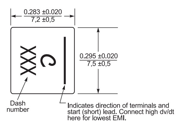
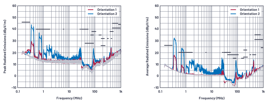
Connecting the side of the inductor with the bar to the high switching node gives the lowest EMI. The image below shows the improvement in radiated emissions when connecting the shortest inductor lead to the switching node.
Solid Reference Planes Under Traces
At high frequencies, the current through a signal trace on a PCB wants to return directly underneath the trace. The best way to achieve this is to ensure there is a reference plane (typically GND) directly below the trace, and there are no gaps or splits in the plane.
The image below shows a example PCB with an upper layer that has a trace on it, and a reference plane on the layer beneath it. A signal source on the bottom left (simulated as a current source here) generates a signal that travels along the trace on the top layer, and returns through the reference plane on the second layer. At DC or low frequencies, the return current takes the shortest path straight through the copper plane back to the source. However at high frequencies the current travels back through the plane on a path that is directly underneath the trace3 4.
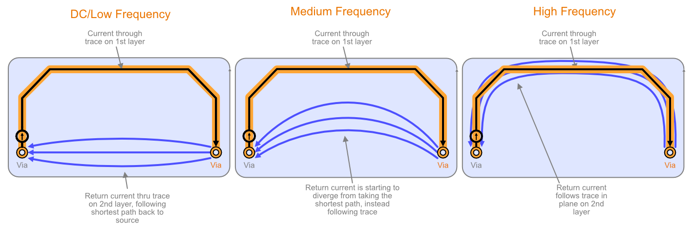
At all frequencies, the return current is taking the path of least impedance (well, distributing itself among all paths, proportional to the inverse of impedance). At low frequencies, this happens to be the shortest path, as the impedance is dominated by the resistance of the copper. At high frequencies, the impedance is dominated by the inductance, and the path of lowest inductance happens to be directly underneath the trace where in minimizes the loop area of the current loop.
The below image shows what happens when there is a gap in the reference plane, preventing the return current from travelling directly underneath the trace. The current has to spread out around the gap, increasing the overall loop area and making the EMI worse.
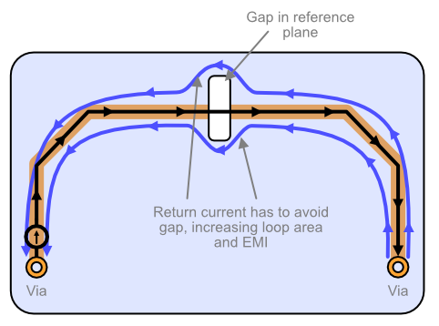
This is why it is important to have continuous reference planes under traces whenever possible. If removing a gap (or split) is impossible, then the next best thing is to bridge the gap on another layer, tying the bridge to the reference plane on each side of the gap.
Contact vs. Non-Contact Probes
Non-contact probes have the advantage of being easy to use. They do not require you to make and break electrical connections to test the circuit. They don’t require you to ground the probe using a very short and obtrusive ground lead. They don’t run the risk of shorting out parts of the circuit if your hand slips (non-contact probes are almost always insulated).
Oscilloscope Probes
The loop made with the probe tip and it’s ground connection forms an unshielded antenna which will pick up high frequency noise in it’s vicinity.
Most general-purpose oscilloscope have very poor common-mode rejection. The common-mode rejection capability of an oscilloscope probe can be gauged by firstly connecting the probe tip and ground together, and then connecting both up a noisy PCB track. Ideally, the oscilloscope waveform should still be a flat line. The more noise seen on the oscilloscope, the poorer the probe’s common-mode rejection.
The impedance mismatch between the noise source, the tracks, the scope probe and oscilloscope may cause reflections to reduce the accuracy of your noise measurements.
For example, the output impedance of a SMPS may be a few , which then connects to the PCB tracks and scope probe, which may have an impedance of . This then connects to the oscilloscope which has an impedance in the .
These reflections can be minimised by adding the appropriate termination resistors, e.g. a resistor in series with the SMPS (as close to the SMPS output as you can), and then another resistor in parallel (shunt to ground), as close to the oscilloscope input as you can. All noise measurements
Mu-metal
Mu-metal is a nickel-iron alloy with a very high permeability, making it suitable for shielding sensitive equipment against magnetic interference.
Footnotes
-
Christian Kueck. Layout for Power Designs #1: Hot Loops. Analog Devices. Retrieved 2022-07-13, from https://www.analog.com/en/technical-articles/layout-for-power-designs-1-hot-loops.html. ↩
-
Keith Szolusha, Gengyao Li, and Frank Wang (2021, Jun). Does the Assembly Orientation of an SMPS Inductor Affect Emissions? [Article]. Analog Devices. Retrieved 2023-07-15, from https://www.analog.com/en/analog-dialogue/articles/does-the-assembly-orientation-of-an-smps-inductor-affect-emissions.html. ↩
-
LearnEMC. Identifying Current Paths [Article]. Retrieved 2023-07-16, from https://learnemc.com/identifying-current-paths. ↩
-
Zm Peterson (2020, Feb 5). How to Design Your PCB Return Current Path [Article]. NWES. Retrieved 2023-07-16, from https://www.nwengineeringllc.com/article/how-to-design-your-pcb-return-current-path.php. ↩