

 NinjaCalc
Gate Drivers

A gate driver is an IC that sits between a logic-level control signal (e.g. a PWM output from a microcontroller) and the gate of a power switch such as a MOSFET, IGBT or GaN/SiC transistor. It provides the large peak currents needed to charge and discharge the gate capacitance quickly, and (depending on the topology) shifts the drive voltage up to a floating high-side source node (or isolates it from the control ground altogether).
Topologies
Low-side Gate Drivers
The drivers will typically accept a wide range of voltage for the VDD pin (the pin the gate will be driven to when going HIGH). They will decouple the logic-level signals from this such that a logic-level input will still be considered HIGH when VDD is say .
Photovoltaic Gate Drivers
Photovoltaic gate drivers use the light energy from an LED to charge a small photovoltaic cell to provide an isolated gate drive voltage. The LED and photovoltaic cell are typically packaged together in a single small IC package (e.g. SOP-4).
They are great for driving MOSFETs across an isolation barrier at low switching speeds, without the need for a separate isolated power supply (all the energy comes from the LED). The trade-off is speed: the photovoltaic cell only sources tens of microamps at most, so charging the gate takes anywhere from microseconds to milliseconds depending on the MOSFET’s gate charge. This makes them suited to static or slow switching (e.g. load disconnects, battery isolation), not PWM at tens of kHz.
Because of their isolation, they are a great choice for driving high-side MOSFETs (and back-to-back MOSFETs) that don’t require high switching speeds. This is because you can tie the V− output to the source of the MOSFET and get a guaranteed positive gate-source voltage on the V+ output no matter what the source voltage is doing. The schematic below illustrates this. Driving a high-side N-channel MOSFET with a ground-referenced logic signal (e.g. ) would not work. The MOSFET would turn on initially, but as soon as the load voltage rises at the source of the MOSFET, the gate-source voltage collapses and the MOSFET would sit in a partially-on state (acting as a source follower, with the source settling at roughly the gate voltage minus ). Driving the gate with () is also not an option: you would get the same problem as the source rises towards . Also, MOSFET gate-source voltages are typically limited to (abs. max.), so this would blow up the MOSFET when the source is low (i.e. at startup).
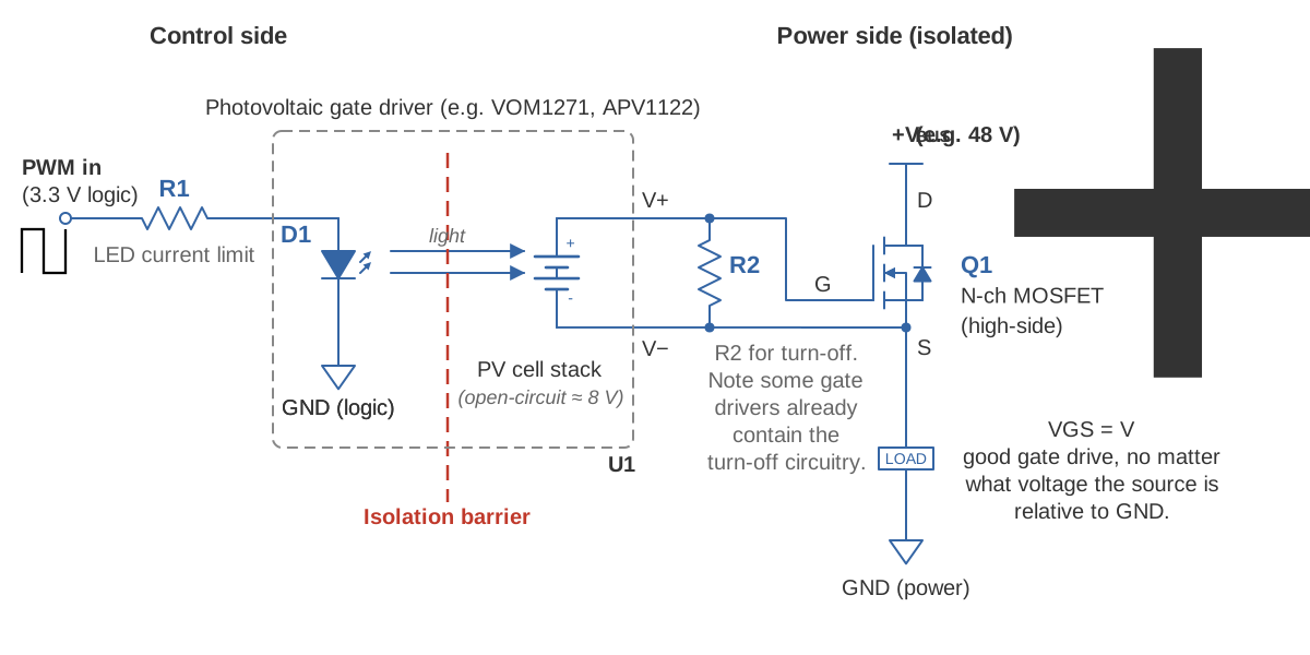
An alternative to a photovoltaic gate driver for high-side N-channel MOSFETs is a bootstrap gate driver. This uses a bootstrap capacitor and diode: the capacitor is charged from the driver’s supply while the switch node (the MOSFET’s source) is low, and then “rides up” with the source to power the floating high-side driver stage. Bootstrap drivers are the normal choice for hard-switched half-bridges at tens of kHz to MHz (e.g. buck converters and motor drives), where the capacitor is refreshed every cycle. The catch is that the switch node has to be pulled low periodically to recharge the capacitor, so a bootstrap driver cannot hold a high-side MOSFET on indefinitely. A photovoltaic gate driver has no such time limit (it can hold the MOSFET on forever), which is the main reason to choose one for slow or static switching.
Another alternative is to just use a P-channel MOSFET for the high-side switch. This is a simple solution and can be driven from voltages within to (although an N-channel MOSFET is usually needed to pull the P-channel gate down if you want to use a logic-level control signal). The downside is that P-channel MOSFETs have higher on-resistance and lower current ratings than N-channel MOSFETs (for the equivalent price and physical size), so they are not as efficient for high-current applications.
Part Recommendations
Texas Instruments UCC2751x
The Texas Instruments UCC2751x is a family of single-channel, high-speed, low-side gate drivers. It is capable of 4 A peak when both sourcing and sinking current to the gate. They are available in SON-6 and SOT-23-5 packages.1
| Parameter | Value |
|---|---|
| VDD | 4.5 V to 18 V |
| Ipeak source/sink | 4 A/4 A |
| Propagation delay | 13 ns (typ.) |
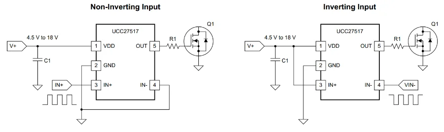
The logic inputs support both TTL and CMOS levels, independent of VDD.
External Resources
- International Rectifier (now Infineon) - Application Note AN-937 - Gate Drive Characteristics And Requirements for HEXFET Power MOSFETs is a great article on gate drive (including isolated gate drive) techniques.
Footnotes
-
Texas Instruments (2014, Dec). UCC27516, UCC27517: Single-Channel, High-Speed, Low-Side Gate Driver (With 4-A Peak Source and 4-A Peak Sink) [datasheet]. Retrieved 2026-09-17, from https://www.ti.com/lit/ds/symlink/ucc27517.pdf. ↩ ↩2