Thermal Design For PCBs
| Date Published: | |
| Last Modified: |
Overview
The resistor model is commonly used to calculate basic PCB operating temperatures.
What Is Thermal Conductivity?
Specific Thermal Conductivity
Specific thermal conductivity is a property of a material which describes it’s ability to conduct heat. Materials with a high specific thermal conductivity conduct heat well, and materials with a low specific thermal conductivity conduct heat poorly (they are called thermal insulators). The symbol \( \lambda \) (lambda) is typically used to represent specific thermal conductivity.
$$\begin{align} \lambda = \frac{P \cdot t}{A \cdot \Delta T} \end{align}$$where:
\( \lambda \) is the specific thermal conductivity in \( W \cdot m^{-1} \cdot K^{-1} \)
\( P \) is the power in \(Watts\)
\( t \) is the thickness, in \(meters\)
\( A \) is the surface area, in \(meters^2\)
\( \Delta T \) is the difference in temperature between the hot and cold surfaces in \(Kelvin\)
Thermal resistance is just the inverse (reciprocal) of thermal conductivity.
Absolute Thermal Conductivity
Absolute thermal conductance is defined as:
$$\begin{align} \lambda_A = \frac{P}{A \cdot \Delta T} \end{align}$$where:
\( \lambda_A \) is the absolute thermal conductivity in \( W \cdot K^{-1} \)
\( P \) is the power in \(Watts\)
\( A \) is the surface area, in \(meters^2\)
\( \Delta T \) is the difference in temperature between the hot and cold surfaces in \(Kelvin\)
Notice how it is very similar to the formula for specific thermal conductivity, except it is missing the thickness \(t\). Care has to be taken to distinguish between the two types of thermal resistances! To recap:
- Specific thermal conductivity is a property of the material, irrespective of it’s shape, length, size, e.t.c. It has units \( W \cdot m^{-1} \cdot K^{-1} \). This is what we were talking about above.
- Absolute thermal conductivity (and absolute thermal resistance) is used when talking about the thermal conductance of a via, copper plane, PCB, e.t.c. This value takes into account both the material and it’s shape/length/size. This has units \( W \cdot C^{-1} \). Absolute thermal resistance is the value mentioned on component datasheets.
However, both of these thermal conductivities are usually referred to without the “specific” or “absolute” qualifier, leaving it up to you to work out what is being used based on the context and units. Remember, 99% of the time when a component datasheet mentioned “thermal resistance” they will be talking about “absolute thermal resistance”.
If you know the specific thermal conductivity, you can find the absolute thermal conductivity with:
$$\begin{align} \lambda_A = \frac{\lambda_A \cdot A}{t} \end{align}$$Below are the specific thermal conductivities for common PCB materials:
| Material | Specific Thermal Conductivity (\(W \cdot m^{-1} \cdot K^{-1}) \) |
|---|---|
| Air | 0.026 |
| Aluminium | 205 |
| Copper | 401 |
| FR-4 | 0.29 (through-plane), 0.81 (across-plane) |
| Rogers 92ML | 2.0 (through-plane) |
| Gold | 314 |
| Silver | 406 |
| Solder, SnAgCu | 58 |
| Soldermask | 0.2 |
| Plating, ENIG | 58 |
| TIM, phase change | 2.23 |
Most of these values were obtained from http://hyperphysics.phy-astr.gsu.edu/hbase/Tables/thrcn.html1. Solder, SnAgCu and Plating, ENIG values sourced from https://www.digikey.co.nz/en/articles/optimizing-pcb-thermal-performance-for-cree-xlamp-leds. TIM, phase change was sourced from https://www.laird.com/thermal-interface-materials/phase-change-materials/tpcm-900.
You can use these values to calculate an absolute thermal resistance for a particular layer in a PCB stack-up. For example, if we wanted to calculate the absolute thermal resistance \( R_\theta \) of a \( 2cm^2 \) area of soldermask that is \( 20um \) thick:
$$\begin{align} R_\theta &= \frac{1}{\lambda_{A}} \\ &= \frac{t}{\lambda \cdot A} \\ &= \frac{20um}{0.2Wm^{-1}K^{-1} \cdot 2cm^2} \\ &= 0.5KW^{-1} \\ &= 0.5°CW^{-1} \end{align}$$Thermal conductivity has some dependence on temperature (especially near \(0K\)), however for most materials at common PCB temperatures the thermal conductivity can be considered constant.
Non-isotropic materials such as FR-4 (which is a glass epoxy) have different thermal conductivities in the through-plane (Z) and across-plane (XY) directions.
ASTM D5470 is a standard used to measure thermal conductivity.
If the thickness of a material is known and constant, sometimes manufacturers will give a thermal resistance with units \( °C \cdot m^2 \cdot W^{-1} \) (or \( °C \cdot in^2 \cdot W^{-1} \)). This is common for areas of FR-4 PCB (when the thickness is defined as say, 1.6mm), or for TIM material with a defined thickness of say 0.1mm. When this is given, they have already taken the thickness \(t\) into account and applied it to the equation. In this sense the thermal resistance is half-way between a specific thermal resistance and an absolute thermal resistance. To fully calculate an absolute thermal resistance from this value, all you need to do is divide the resistance by the area of the material:
$$\begin{align} R_\theta = \frac{R_{\theta, °Cm^2W^{-1}}}{A} \end{align}$$The Thermal Resistor Model
Remember, thermal resistance is the inverse of thermal conductance. When modelling the thermal properties of PCBs, it is useful to use thermal resistance instead of conductance as the resistances sum when the materials are in series, just like resistance values would. We use absolute thermal resistances here as we have taken into account the thickness.
Just like resistance is defined via Ohm’s law as \( R = \frac{V}{I} \), thermal resistance (absolute) \(R_\theta\) is defined as:
$$\begin{align} R_{\theta} = \frac{\Delta T}{P} \end{align}$$where:
\( R_\theta \) is the thermal resistance, in \( °C \cdot W^{-1} \)
\( \Delta T \) is the difference in temperature, in \(°C\)
\( P \) is the power dissipation, in \( W \)
When talking about thermal resistances, a resistor symbol is used to indicate the fixed thermal resistance of a component or piece of hardware, between two points or two surfaces. The difference in temperature is analogous to the voltage drop across a resistor, and the power dissipation is analogous to the current through the resistor.

When looking through component datasheets, one of the most common thermal resistances is the junction-to-ambient thermal resistance. This value is defined as:
$$\begin{align} \theta_{JA} = \frac{T_J - T_A}{P} \end{align}$$where:
\( T_J \) is the temperature at the junction (the silicon die) inside the IC, in \(°C\)
\( T_A \) is the ambient temperature (temperature of air/environment PCB is in), in \(°C\)
\( P \) is the power dissipation of the IC, in \(W\)
However, you have to be vigilant with specified junction-to-ambient values as they are not just a property of the component package, but also of the PCB! When specified on a datasheet it is usually tested on a JEDEC standardized PCB and package land pattern.
A much more useful thermal resistance in a components datasheet is the junction-to-case thermal resistance. This is usually specified as \( \theta_{JC} \). This typically represents the thermal resistance from the junction to the place on the PCB where the component is soldered. You can then take into account your PCB layout and estimate a case-to-ambient thermal resistance.

A diagram of the different temperature points used when defining thermal resistances for ICs mounted on PCBs.
Your case-to-ambient thermal resistance can be added to the manufacturer-specified junction-to-case thermal resistance to get the total junction-to-ambient resistance using simple addition:
$$\begin{align} \theta_{JA} = \theta_{JC} + \theta_{CA} \end{align}$$The Thermal Resistance Of A Via
Thermal vias are a very common way of dissipating heat away from an IC or other component. They are normally placed in and around the thermal pad of a component package. However, via-in-pads cause solder wicking issue. During the soldering process, both gravity and surface tension can push molten solder down the barrel of a via, sucking solder away from the pad. This can leave a pad which is under-soldered and a dry joint. Unfortunately, you cannot even rely on the solder wicking to completely “plug” a via, which would be advantageous in certain circumstances (it would decrease the thermal resistance of the vias). Instead, the via barrel typically only gets partially filled and has “voids” of air.
There are a few ways to prevent wicking:
- 0.3mm or smaller via diameter limits the amount of solder wicking that will occur.
Adding more thermal vias is a case of dimensioning returns, due to the limited spreading of the heat in the horizontal direction.
Via Thermal Resistance Calculator
Copper Planes
(2oz.) copper is recommended for top and bottom layers.
Thermal Interface Material (TIM)
Thermal interface materials (TIMs) are thin layers of compressible (“compliant”) thermally conductive material that are used to provide good thermal coupling between two components. They are usually used between a PCB and a heatsink. Both the PCB and heatsink are made of hard materials that although they look flat, contain microscopic rough patches which when sandwiched together, create insulating air gaps and make the heatsinking inadequate. Inserting a thin TIM between the PCB and heatsink removes these air gaps and greatly reduces the thermal resistance of the system. Many TIMs try to be as thermally conductive as possible while being an electrical insulator (if only diamond was cheap enough!).
- Thermal grease TIMs: Offers the best thermal conductivity, but can be messy and slow to apply.
- Phase-change TIMs: Have a high thermal conductivity but require significant clamping force for correct operation.
- Adhesive-based TIMs: Have the lowest thermal conductivity but require less clamping force.
Phase-change TIMs are a flexible solid sheet at room temperature, but quickly soften at higher temperatures (e.g. 50°C and above) to fill in microscopic irregularities between the two surfaces and decrease thermal resistance. The thickness of phase-change TIMs is usually between 0.1 and 0.5mm. Boron nitride is an example of a compound which has phase-change abilities.
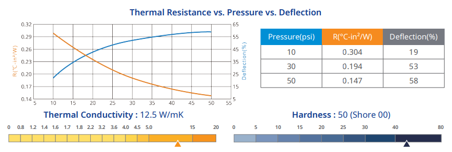
The relationship between pressure and thermal resistance for a silicon TIM from T-Global Technology (TG-A1250). Image acquired 2020-08-14 from http://www.tglobaltechnology.com/uploads/files/tds/TG-A1250.pdf.
References
http://hyperphysics.phy-astr.gsu.edu/hbase/Tables/thrcn.html. Visited 2020-08-10. ↩︎
Authors


This work is licensed under a Creative Commons Attribution 4.0 International License .
Related Content:
Tags
- PCB design
- thermal design
- junction
- ambient
- temperature
- power dissipation
- resistor model
- thermal resistance
- thermal conductivity
- vias
- calculator
- specific thermal conductance
- specific thermal resistance
- absolute thermal conductance
- absolute thermal resistance
- thermal interface material
- TIM
- phase change