Current Sources And Sinks
| Date Published: | |
| Last Modified: |
Overview
Current sources and current sinks are electronic circuits which allow a fixed amount of current to flow through it, irrespective of the voltage across it. A current source (or sink) is not a single passive component, but a small circuit usually made from an active element (transistor, op-amp) and a few passives (such as resistors). Current sources/sinks are used as a sub-circuit in many larger circuit designs.
Uses of current sources:
- Driving LEDs (especially high power LEDs).
- Biasing resistors for pull-ups/pull-downs.
- Charging capacitors to provide a linear increase in voltage across it (e.g. to make a sawtooth or triangular waveform).
Current sources are very common in circuit design, and as such are usually drawn using schematic symbols as shown below. An independent current source is once which has a predetermined fixed set current. A controlled (or dependent) current source is one which is determined by another measurable value in the circuit, usually a voltage (e.g. \(I_{source} = kV_{\text{somewhere else}}\)). You may have seen a controlled current source symbol in the small-signal model for a BJT. Many analogue IC functional diagrams will show current sources with these symbols, hiding the discrete components they are made from.

The compliance of a current source is the voltage range that the current source can operate over and function correctly. Outside of this range, either components are damaged (maximum voltage ratings are exceeded) or the current falls out of regulation.
Current sources may either provide power into a circuit (like a power supply), or require external power to operate.
Zener Diode And BJT Current Source
Below shows one of the popular methods for constructing a current source from a Zener diode and BJT.

How It Works
. The Zener diode \(D1\), biased into it’s voltage regulation range with resistor \(R1\), maintains a steady voltage \(V_B\) at the base of the BJT transistor. . Using the rule that there is a \(0.7V\) drop the base-emitter junction of a BJT, this puts a fixed voltage at the emitter also. . Since this means there is a fixed voltage across \(R_E\), this means by Ohm’s law there is a fixed current through \(R_E\). . Because most of the current supplied to the emitter of a BJT comes from the collector (only about 100-800th of the current comes from the base, depending on the gain \(h_{FE}\) of the BJT), this means there is a fixed current through \(R_{load}\) also!
The current through the load is given by:
$$\begin{align} I_{load} = \frac{V_Z - 0.7V}{R_E} \end{align}$$where:
\(V_Z\) is the voltage of the Zener diode in \(V\)\(R_E\) is the resistance of resistor \(R_E\) in \(\Omega\)\(I_{load}\) is the resulting current through the load resistor, in \(A\)
Constant-Current Diode (JFET Current Source)
The constant-current diode (a.k.a JFET current source, current-limiting diode (CLD), or regulating diode1) is a very simple current source made from a JFET and optional resistor.
Below shows the schematic for a constant-current diode:
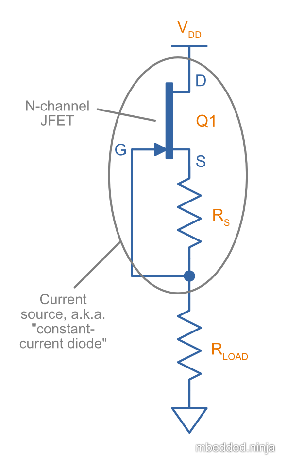
Schematic for a constant-current diode, a.k.a JFET current source. Current source is very simple, and consists of just an N-channel JFET and (optional) resistor. This two-terminal current source is not referenced to any rail and thus the load can be high-side, low-side, or anywhere in-between!
How It Works
The constant-current diode works by using the resistor \(R_S\) to negatively bias the N-channel JFET at a specific operating point. At this operating point the current from drain to source (and consequentially the load) will be relatively constant2.
TIP: Because of the typically large \(R_S > 100\Omega\) this circuit is only suitable for making low-power current sources up to the \(10mA-100mA\) range. Also, because of the large uncertainty in \(V_{GS(off)}\) (e.g. for the 2N5457, the datasheet says it is somewhere between \(-0.5V\) and \(-6.0V\)!3), these don’t make very accurate current sources (without trimming). But they are stable!
How To Calculate The Value Of The Resistor \(R_S\)
Decide on what N-channel JFET you are going to use and your desired constant current, \(I_D\).
You then calculate the required gate-source voltage4:
$$\begin{align} \label{eq:jfet-vgs} V_{GS} = V_{GS(off)} \left[ 1 - (\frac{I_D}{I_{DSS}})^{1/k} \right] \end{align}$$where:\(V_{GS}\) is the gate-source voltage required to bias the JFET at the correct current, in \(V\)\(V_{GS(off)}\) is the gate-source cutoff voltage, a parameter you can get from the JFETs datasheet, in \(V\)\(I_D\) is the current you want the current source to drive at, in \(A\)\(I_{DSS}\) is the zero gate-source drain current, a parameter you can get from the JFETs datasheet, in \(A\)\(k\) is the conduction parameter for the JFET, and depends on the device geometry. This is not normally mentioned in the datasheet, however for this equation you can generally assume it to be \(2\).
You can then find the value of \(R_S\) with:
$$\begin{align} \label{eq:rs-vgs-id} R_S = \frac{|V_{GS}|}{I_D} \end{align}$$
Worked Example: 1.0mA Constant-Current Diode
Let’s design a constant-current diode using the ubiquitous 2N5457 JFET (we’ll choose the one from On Semi) for a constant current \(I_D\) of \(1.0mA\).
From the OnSemi 2N5457 datasheet, we get the following values:
$$\begin{align} I_{DSS} &= 3.0mA\ \text{(typ)} \\ V_{GS(off)} &= -6.0V\ \text{(max)} \\ \end{align}$$Plugging these values into \(Eq.\ \ref{eq:jfet-vgs}\) we can work out the required gate-source voltage (with the common assumption that \(k = 2\)):
$$\begin{align} V_{GS} &= V_{GS(off)} \left[ 1 - (\frac{I_D}{I_{DSS}})^{1/k} \right] \nonumber \\ &= -6.0V \left[ 1 - (\frac{1.0mA}{3.0mA})^{1/2} \right] \nonumber \\ &= -2.54V \end{align}$$Knowing the current \(I_D\) through the resistor and the voltage \(V_{GS}\) across it, we can find the resistance using \(Eq.\ \ref{eq:rs-vgs-id}\):
$$\begin{align} R_S &= \frac{V_{GS}}{I_D} \nonumber \\ &= \frac{|-2.54V|}{1.0mA} \nonumber \\ &= 2.54k\Omega \\ \end{align}$$Done!
The resistor \(R_S\) can be replaced with a potentiometer to create a variable current source, or for tuning/calibration of the current source to a precise value (typically a trimmer-style potentiometer would be used for this).
An important parameter determining the accuracy/stability of a constant-current diode is the output conductance \(g_{oss}\) of the JFET. This is the ratio of change in \(I_D\) to change in \(V_{DS}\). This is a measure of how stable the constant-current source will be to changes in the voltage across it, which occur if either the supply voltage or load resistance changes. The lower the \(g_{oss}\) the better (an ideal current source would have \(g_{oss} = 0\), which is the equivalent to a resistance of \(\infty\)).
For more great reading on the constant-current diode, see https://www.vishay.com/docs/70596/70596.pdf.
Depletion-Mode MOSFET Current Source
TODO: Add info.
Op-amp Current Sink
The following schematic shows such a device which can control between 0-1A through the load (shown as \(R_{load}\)):
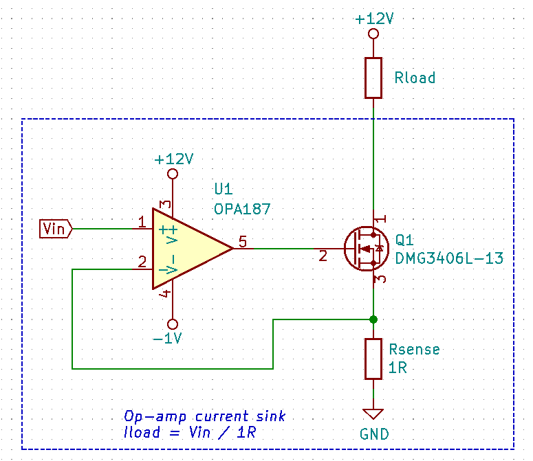
You set the desired load current by providing a voltage to \(V_{in}\). This voltage typically comes from a resistor divider (fixed current), potentiometer (manually variable current) or DAC (digitally variable current). The load current is given by the simple Ohm’s law equation:
$$\begin{align} I_{load} = \frac{V_{in}}{R_{sense}} \end{align}$$The circuit works like this:
. Desired voltage to set current is provided to \(V_{in}\) which is applied to the positive input of the op-amp, \(V_{op+}\). . The op-amp will then drive it’s output high in an attempt to bring it’s \(V_{op-}\) to the same voltage. . As the op-amp raises the voltage on it’s output, this is connected to the gate of the MOSFET, which will begin to turn it on. . As the MOSFET turns on, current begins to flow through the load and sense resistor, \(R_{sense}\). . The op-amp will keep turning the MOSFET on until the voltage drop across \(R_{sense}\) is equal to \(V_{in}\), meaning \(V_{op-}\) is the same as \(V_{op+}\). . This voltage drop will occur when we have the desired amount of current flowing through it, leading to the equation \( I_{load} = \frac{V_{in}}{R_{sense}} \).
Things to note:
- The op-amp is powered here with a slightly negative voltage rail on it’s \(V_{SS}\) pin. This is that the op-amp remains operational when you set it at low current levels. At low current levels, the voltages at \(V_{op+}\) and \(V_{op-}\) are very close to zero. Even rail-to-rail op-amps can have trouble performing well if the negative voltage rail was at \(0V\).
- The power dissipation through the MOSFET and sense resistor has to be considered. The sense resistor is easy, just make sure it can handle the power given by \(P = I^2 R\) at the maximum current. The MOSFET power dissipation will depend on the load current and voltage drop across it. The MOSFET is used in it’s active region — the region where it is not fully on nor fully off. The MOSFET will drop the remaining voltage from the voltage source provided to the load, once the load voltage drop and sense resistor voltage drop has been subtracted. Use the equation \(P = VI\) to determine the power dissipation in the MOSFET.
- The gate capacitance of the MOSFET can load the op-amp output to the point that it introduces enough phase lag to cause the circuit to go unstable. See below to recommended compensation circuitry to add to the basic schematic to make the design more stable.
Current Sinking Accuracy
The accuracy of the current sink primarily depends of three aspects:
- The input offset voltage of the op-amp.
- The accuracy of the DAC (or other voltage source) providing the voltage to \(V_{in}\).
- The tolerance of the current-sense resistor.
MOSFET Gate Capacitance Compensation
The gate capacitance of the MOSFET can load the op-amp output to the point that it introduces enough phase lag to cause the circuit to go unstable. Compensation circuitry can be added as shown in the below circuit to limit the phase lag and prevent the circuit from becoming unstable.
![A schematic showing gate capacitance compensation circuitry on a op-amp based current sink using the LT1492[^bib-linear-lt1492-ds].](https://blog.mbedded.ninja/electronics/components/current-sources-and-sinks/lt1492-voltage-controlled-current-sink.png)
A schematic showing gate capacitance compensation circuitry on a op-amp based current sink using the LT14925.
Read https://electronics.stackexchange.com/questions/69506/stability-problem-in-unity-gain-opamp for more information.
References
Central Semiconductor Corp.. What is a Current Limiting Diode?. Retrieved 2022-01-11, from https://www.centralsemi.com/pdfs/selection/leaded/what_is_a_cld.pdf. ↩︎
Electronics Tutorials. FET Current Source. Retrieved 2022-01-11, from https://www.electronics-tutorials.ws/transistor/fet-current-source.html. ↩︎
On Semiconductor (now On Semi) (2010, Feb). 2N5457, 2N5458 JFETs: General Purpose N−Channel − Depletion (datasheet). Retrieved 2022-01-11, from https://www.onsemi.com/pdf/datasheet/2n5457-d.pdf. ↩︎
Siliconix (now Vishay) (1997, Mar 10). AN103: The FET Constant-Current Source/Limiter. Retrieved 2021-04-29, from https://www.vishay.com/docs/70596/70596.pdf. ↩︎
Linear Technology. LT1492/LT1493: 5MHz, 3V/µs, Low Power Single Supply, Dual and Quad Precision Op Amps (datasheet). Retrieved 2020-12-25 from https://www.analog.com/media/en/technical-documentation/data-sheets/14923f.pdf. ↩︎
Authors


This work is licensed under a Creative Commons Attribution 4.0 International License .
Related Content:
- Shift Registers
- Peltiers (Thermoelectric Cooler)
- Electropermanent Magnets (EPMs)
- Neon Sign Transformers
- PROFIBUS